
Page 165 - Semiconductor Manufacturing Handbook
P. 165
Geng(SMH)_CH12.qxd 04/04/2005 19:49 Page 12.14
PLASMA ETCHING
12.14 WAFER PROCESSING
of polymer is deposited during a deposition step. However,
if the polymer removal rate is controlled so that it is rela-
tively independent of AR, the time required to clear the
polymer at the bottom of trench A will be shorter. So trench
A will have an early start in the isotropic etching process.
Despite a slower isotropic etch rate in trench A, the result-
ing etch depth in it could be the same as that in trench B by
the time a deposition/etch cycle finishes.
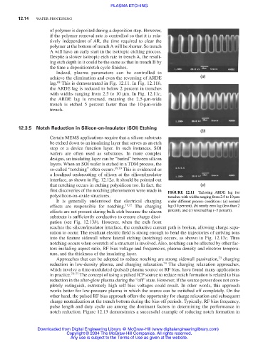
Indeed, plasma parameters can be controlled to
achieve the elimination and even the reversing of ARDE (a)
68
lag. This is demonstrated in Fig. 12.11. In Fig. 12.11b,
the ARDE lag is reduced to below 2 percent in trenches
with widths ranging from 2.5 to 10 µm. In Fig. 12.11c,
the ARDE lag is reversed, meaning the 2.5-µm-wide
trench is etched 5 percent faster than the 10-µm-wide
trench.
12.3.5 Notch Reduction in Silicon-on-Insulator (SOI) Etching
(b)
Certain MEMS applications require that a silicon substrate
be etched down to an insulating layer that serves as an etch
stop or a device function layer. In such instances, SOI
wafers are often used as substrates. In more complex
designs, an insulating layer can be “buried” between silicon
layers. When an SOI wafer is etched in a TDM process, the
so-called “notching” often occurs. 69,70 This is evidenced as
a localized undercutting of silicon at the silicon/insulator
interface, as shown in Fig. 12.12a. It should be pointed out
that notching occurs in etching polysilicon too. In fact, the (c)
first discoveries of the notching phenomenon were made in
FIGURE 12.11 Tailoring ARDE lag for
polysilicon-on-oxide structures. trenches with widths ranging from 2.5 to 10 µm
It is generally understood that electrical charging under different process conditions: (a) normal
effects are responsible for notching. 71,72 The charging lag (10 percent), (b) nearly zero lag (less than 2
effects are not present during bulk etch because the silicon percent), and (c) reversed lag (−5 percent).
substrate is sufficiently conductive to ensure charge dissi-
pation (see Fig. 12.13b). However, when the etch front
reaches the silicon/insulator interface, the conductive current path is broken, allowing charge sepa-
ration to occur. The resultant electric field is strong enough to bend the trajectories of arriving ions
into the feature sidewall where lateral etching (notching) occurs, as shown in Fig. 12.13c. Thus
notching occurs when overetch of a structure is involved. Also, notching can be affected by other fac-
tors including aspect ratio, RF bias voltage and frequencies, plasma density and electron tempera-
ture, and the thickness of the insulating layer.
73
Approaches that can be adopted to reduce notching are strong sidewall passivation, charging
reduction in low-density plasma, and charging relaxation. 74 The charging relaxation approaches,
which involve a time-modulated (pulsed) plasma source or RF bias, have found many applications
in practice. 75–77 The concept of using a pulsed ICP source to reduce notch formation is related to bias
reduction in the after-glow plasma during the “off” state. However, if the source power does not com-
pletely extinguish, extremely high self bias voltages could result. In other words, this approach
works better for low-pressure plasma in which the source can be switched off completely. On the
other hand, the pulsed RF bias approach offers the opportunity for charge relaxation and subsequent
charge neutralization at the trench bottom during the bias off periods. Typically, RF bias frequency,
pulse length and duty cycle are among the dominant factors in determining the performance in
notch reduction. Figure 12.13 demonstrates a successful example of reducing notch formation in
Downloaded from Digital Engineering Library @ McGraw-Hill (www.digitalengineeringlibrary.com)
Copyright © 2004 The McGraw-Hill Companies. All rights reserved.
Any use is subject to the Terms of Use as given at the website.