
Page 160 - Semiconductor Manufacturing Handbook
P. 160
Geng(SMH)_CH12.qxd 04/04/2005 19:49 Page 12.9
PLASMA ETCHING
PLASMA ETCHING 12.9
12.3.1 Time Division Multiplex Etch Process
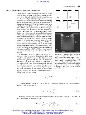
Conventionally, single-step plasma etch processes cannot
simultaneously meet the requirements described previ-
ously. So for silicon-based MEMS device manufacturing, (a) (b)
time division multiplex (TDM) etch processes have been
developed. 54,55 TDM etch processes employ alternating
plasma deposition and etching steps. In deposition steps,
octofluorocyclobutane (C F ) is used and in etching steps
4 8
sulfurhexafluoride (SF ) is used. As shown schematically
6
in Fig. 12.5a–d, during an etching step, free F atoms pro- (c) (d)
mote isotropic and spontaneous reaction with silicon.
During a deposition step, C F plasma promotes Teflon-
4 8
like polymer passivation on all surfaces. In the subsequent
etching step, on directional energetic ion bombardment,
the polymer film formed at the bottom of the etched struc- Mask
tures will be preferentially removed to expose the silicon
surface for further etching, while passivation on the side-
walls remains to inhibit lateral etching. A TDM etch Si
process employs the alternating deposition and etching
steps in a repetitive fashion. This approach allows high-
aspect-ratio features to be defined into silicon substrates at
high etch rates. Figure 12.5e exhibits a cross-sectional (e)
scanning electron microscope (SEM) image of etched Si
trenches.
A simplified physical model can be used to FIGURE 12.5 Schematic illustration of TDM
describe a TDM process. As shown in Fig. 12.6, for a etch processes: (a) A Si wafer with patterned
complete deposition/etch cycle, the deposition step mask, (b) an etching step in which F radicals
facilitate isotropic etching, (c) a deposition step
lasts for time t and the etch step for t . In the deposi- in which polymer forms on all surfaces, (d) a
1
2
tion step, a thin layer of polymer with a thickness of subsequent etching step in which the polymer at
a ⋅t is deposited, where the deposition rate is denoted the horizontal surface is preferentially removed
1 1
as a . In the etch step, however, the first portion of subject to direct ion bombardment, and (e) a
1
time is spent in removing this layer of deposited poly- cross-sectional SEM image of Si trenches etched
mer from the bottom of the feature. If the polymer in a TDM process.
removal rate is a , the time left for further etching of
2
silicon in the etch step is then
at ⋅
t = t − 1 1 (12.1)
2
a 2
Given the isotropic silicon etch rate a , the etch depth achieved during this complete deposi-
3
tion/etch cycle is expressed as
at ⋅
L = a t ⋅ = t − 1 1 (12.2)
a
3
3 a ⋅ 2
2
Assuming the three rates are independent of the depth of etch features, the overall TDM etch rate
in a TDM process is then expressed as
t −
1
1
R = a t ⋅ ⋅ t + 1 t 2 = a ⋅ 2 at ⋅ ⋅ t + 1 t 2 (12.3)
a
3
3
2
1
1
Downloaded from Digital Engineering Library @ McGraw-Hill (www.digitalengineeringlibrary.com)
Copyright © 2004 The McGraw-Hill Companies. All rights reserved.
Any use is subject to the Terms of Use as given at the website.