
Page 159 - Semiconductor Manufacturing Handbook
P. 159
Geng(SMH)_CH12.qxd 04/04/2005 19:49 Page 12.8
PLASMA ETCHING
12.8 WAFER PROCESSING
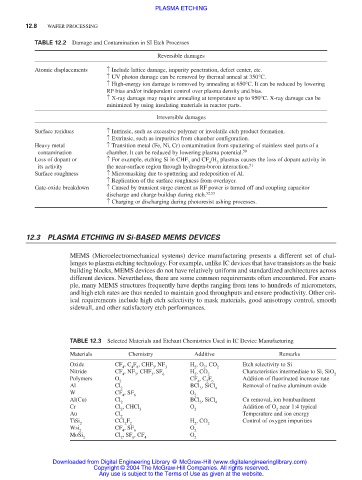
TABLE 12.2 Damage and Contamination in SI Etch Processes
Reversible damages
Atomic displacements ↑ Include lattice damage, impurity penetration, defect center, etc.
↑ UV photon damage can be removed by thermal anneal at 350°C.
↑ High-energy ion damage is removed by annealing at 650°C. It can be reduced by lowering
RF bias and/or independent control over plasma density and bias.
↑ X-ray damage may require annealing at temperature up to 950°C. X-ray damage can be
minimized by using insulating materials in reactor parts.
Irreversible damages
Surface residues ↑ Intrinsic, such as excessive polymer or involatile etch product formation.
↑ Extrinsic, such as impurities from chamber configuration.
Heavy metal ↑ Transition metal (Fe, Ni, Cr) contamination from sputtering of stainless steel parts of a
contamination chamber. It can be reduced by lowering plasma potential. 50
Loss of dopant or ↑ For example, etching Si in CHF and CF /H plasmas causes the loss of dopant activity in
3 4 2
its activity the near-surface region through hydrogen-boron interaction. 51
Surface roughness ↑ Micromasking due to sputtering and redeposition of Al.
↑ Replication of the surface roughness from overlayer.
Gate-oxide breakdown ↑ Caused by transient surge current as RF power is turned off and coupling capacitor
discharge and charge buildup during etch. 52,53
↑ Charging or discharging during photoresist ashing processes.
12.3 PLASMA ETCHING IN Si-BASED MEMS DEVICES
MEMS (Microelectromechanical systems) device manufacturing presents a different set of chal-
lenges to plasma etching technology. For example, unlike IC devices that have transistors as the basic
building blocks, MEMS devices do not have relatively uniform and standardized architectures across
different devices. Nevertheless, there are some common requirements often encountered. For exam-
ple, many MEMS structures frequently have depths ranging from tens to hundreds of micrometers,
and high etch rates are thus needed to maintain good throughputs and ensure productivity. Other crit-
ical requirements include high etch selectivity to mask materials, good anisotropy control, smooth
sidewall, and other satisfactory etch performances.
TABLE 12.3 Selected Materials and Etchant Chemistries Used in IC Device Manufacturing
Materials Chemistry Additive Remarks
Oxide CF , C F , CHF ,NF H , O , CO Etch selectivity to Si
4 4 8 3 3 2 2 2
Nitride CF , NF , CHF ,SF H , CO Characteristics intermediate to Si, SiO
4 3 3 6 2 2 2
Polymers O CF , C F Addition of fluorinated increase rate
2 4 2 6
Al Cl BCl , SiCl Removal of native aluminum oxide
2 3 4
W CF , SF O
4 6 2
Al(Cu) Cl BCl , SiCl Cu removal, ion bombardment
2 3 4
Cr Cl , CHCl O Addition of O near 1:4 typical
2 3 2 2
Au Cl Temperature and ion energy
2
TiSi CCl F H , CO Control of oxygen impurities
2 2 2 2 2
Wsi CF , SF O
2 4 6 2
MoSi Cl , SF , CF O
2 2 6 4 2
Downloaded from Digital Engineering Library @ McGraw-Hill (www.digitalengineeringlibrary.com)
Copyright © 2004 The McGraw-Hill Companies. All rights reserved.
Any use is subject to the Terms of Use as given at the website.