
Page 155 - Semiconductor Manufacturing Handbook
P. 155
Geng(SMH)_CH12.qxd 04/04/2005 19:49 Page 12.4
PLASMA ETCHING
12.4 WAFER PROCESSING
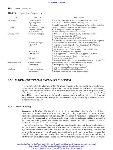
TABLE 12.1 Plasma Etcher Classifications
Criteria Categories Descriptions
Frequency Low frequencies ↑ <1 MHz. Matching network is needed to adapt impedance.
High frequencies ↑ <40 MHz. 13.56 MHz is the most widely used.
Microwave ↑ Usual frequency is 2.45 GHz. Stub tuner is often used for matching.
Pressure Ultralow (≤0.1 mTorr) Diffusion pumps, cryopumps, and turbo pumps are required.
Low (≤100 mTorr) Turbo pumps and blowers are required.
High (> 100 mTorr) Mechanical pumps and blowers are required.
External source Capacitively coupled ↑ With one or more electrodes, and “L” matching network.
−3
↑ Plasma density limited to <10 m .
16
↑ Preferred pressure range of 100–1000 mTorr.
↑ No independent control of plasma density and bias in diode systems.
Inductively coupled ↑ RF coils separated by dielectric wall. L-C matching network.
(ICP) 13–16 ↑ Frequencies in the range of 1–40 MHz, pressure 1–100 mtorr.
17
−3
↑ High-density plasma, n ≥ 10 m .
e
↑ Independent control of plasma source power and bias power.
Wave (ECR, 17 ↑ External DC magnetic field required.
Helicon 18,19 ) ↑ ECR: Typical freq 2.45 GHz; Helicon: typical 13.56 MHz.
↑ ECR: matching usually with a three-stub tuner.
DC bias ↑ Most in ion beam etching .
20
21
↑ Bias applied to conducting materials in high-frequency discharge .
Substrate vicinity Closely coupled Substrate to be etched is placed directly in the plasma.
Downstream ↑ Wafers placed away from plasma region.
22
↑ Used to minimize plasma charging damage .
Load size Single wafer etcher ↑ Each wafer is etched in identical environment.
Batch systems ↑ Multiple wafers are processed simultaneously.
12.2 PLASMA ETCHING IN SILICON-BASED IC DEVICES
Plasma etching has the advantage of faithful pattern transfer in the manufacturing of modern inte-
grated circuit (IC) devices as the critical dimensions of the devices have shrunk to the submicron
regime. Over the last two decades, there have been widespread applications of the plasma etching
technology in making IC devices, along with tremendous progress in the plasma etching technology
itself. This section surveys some of the prevalent aspects, among which are etch rate, etch direction-
ality, selectivity, uniformity and damage, and contamination, in plasma etching of materials involved
in mainstream IC devices.
12.2.1 Silicon Etching
Anisotropy of Etching. Etching of silicon can be accomplished using F-, Cl-, and Br-based
chemistries as the etch products are volatile SiF , SiCl , and SiBr , respectively. For Cl- and Br-based
4
4
4
chemistries, anisotropic plasma etching is caused by the action of neutral gas-solid reactions, which
is stimulated by directional ion bombardment. In other words, ion-enhanced etching is responsible
for anisotropic etching results. For F-based chemistries, however, an inhibitor-assisted mechanism
needs to be involved to achieve anisotropy.
Ion-driven anisotropy. The plasma sheath bias propels positive ions onto the substrate at normal
incidence. Under appropriate conditions, this kind of ion bombardment stimulates anisotropic etch-
ing. It is also important to realize that ions play yet another critical role in Si etching—the reactions
between the substrate and neutral species are significantly accelerated by ion bombardment. For
example, at room temperature chlorine alone does not etch silicon, and the sputtering etch rate by
+
+
Ar too is very small. However, in a plasma where both energetic Ar ions and free Cl atoms are present,
Downloaded from Digital Engineering Library @ McGraw-Hill (www.digitalengineeringlibrary.com)
Copyright © 2004 The McGraw-Hill Companies. All rights reserved.
Any use is subject to the Terms of Use as given at the website.