
Page 158 - Semiconductor Manufacturing Handbook
P. 158
Geng(SMH)_CH12.qxd 04/04/2005 19:49 Page 12.7
PLASMA ETCHING
PLASMA ETCHING 12.7
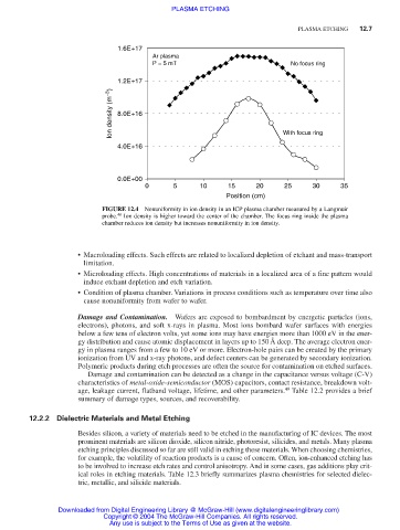
1.6E+17
Ar plasma
P = 5 mT No focus ring
1.2E+17
Ion density (m −3 ) 8.0E+16
4.0E+16 With focus ring
0.0E+00
0 5 10 15 20 25 30 35
Position (cm)
FIGURE 12.4 Nonuniformity in ion density in an ICP plasma chamber measured by a Langmuir
probe. 48 Ion density is higher toward the center of the chamber. The focus ring inside the plasma
chamber reduces ion density but increases nonuniformity in ion density.
• Macroloading effects. Such effects are related to localized depletion of etchant and mass-transport
limitation.
• Microloading effects. High concentrations of materials in a localized area of a fine pattern would
induce etchant depletion and etch variation.
• Condition of plasma chamber. Variations in process conditions such as temperature over time also
cause nonuniformity from wafer to wafer.
Damage and Contamination. Wafers are exposed to bombardment by energetic particles (ions,
electrons), photons, and soft x-rays in plasma. Most ions bombard wafer surfaces with energies
below a few tens of electron volts, yet some ions may have energies more than 1000 eV in the ener-
gy distribution and cause atomic displacement in layers up to 150 Å deep. The average electron ener-
gy in plasma ranges from a few to 10 eV or more. Electron-hole pairs can be created by the primary
ionization from UV and x-ray photons, and defect centers can be generated by secondary ionization.
Polymeric products during etch processes are often the source for contamination on etched surfaces.
Damage and contamination can be detected as a change in the capacitance versus voltage (C-V)
characteristics of metal-oxide-semiconductor (MOS) capacitors, contact resistance, breakdown volt-
49
age, leakage current, flatband voltage, lifetime, and other parameters. Table 12.2 provides a brief
summary of damage types, sources, and recoverability.
12.2.2 Dielectric Materials and Metal Etching
Besides silicon, a variety of materials need to be etched in the manufacturing of IC devices. The most
prominent materials are silicon dioxide, silicon nitride, photoresist, silicides, and metals. Many plasma
etching principles discussed so far are still valid in etching these materials. When choosing chemistries,
for example, the volatility of reaction products is a cause of concern. Often, ion-enhanced etching has
to be involved to increase etch rates and control anisotropy. And in some cases, gas additions play crit-
ical roles in etching materials. Table 12.3 briefly summarizes plasma chemistries for selected dielec-
tric, metallic, and silicide materials.
Downloaded from Digital Engineering Library @ McGraw-Hill (www.digitalengineeringlibrary.com)
Copyright © 2004 The McGraw-Hill Companies. All rights reserved.
Any use is subject to the Terms of Use as given at the website.