Page 162 - Semiconductor Manufacturing Handbook
P. 162
Geng(SMH)_CH12.qxd 04/04/2005 19:49 Page 12.11
PLASMA ETCHING
PLASMA ETCHING 12.11
at sidewall. Although this approach reduces scalloping, it is at the expense of the overall feature pro-
file. Oxide or nitride passivation layers are typically very thin, leading to difficulties in controlling
the profile. Also, oxygen-scavenger gases (such as CHF , C F , and CF ) need to be added to the
3 4 8 4
plasma to minimize oxide formation on the etch front to obtain the desired overall etch rate.
An alternative approach to minimize scallop formation is to use shorter etch steps. 56,58 Keep in
mind, however, that in TDM etch processes, different gases are introduced into a reactor at different
flow rates and chamber pressures are maintained at different levels as required. For example, in etch
steps, etchant gas SF is introduced into the reactor and C F gas is excluded from it; in deposition
6 4 8
steps, C F gas is introduced into the reactor and SF gas should be excluded. Such abrupt gas
4 8 6
changes are often not smooth and cause plasma instability. A fast gas switching technique has been
59
developed to alleviate this problem. The gas switching technique, in combination with a technique
controlling pressure alternations, eliminates the destabilizing pressure “burst” even when very short
process cycles, that is, <1 s, are used.
The challenge here is to minimize scallop dimensions while maintaining TDM etch rates. Again,
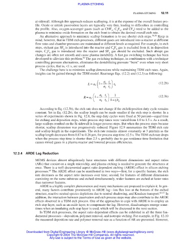
insights can be gained through the TDM model. Rearrange Eqs. (12.2) and (12.3) as following:
a t
L = a ⋅ 1 − 1 ⋅ 1 t ⋅ (12.2b)
3 a t 2
2
2
a t 1
R = a ⋅ 1 − 1 ⋅ 1 ⋅ (12.3b)
3
a 2 t 1 + tt /
2
12
According to Eq. (12.3b), the etch rate does not change if the etch/deposition duty cycle remains
constant. Yet in Eq. (12.2b), the scallop length can be made smaller if the etch step is shorter. In a
series of experiments shown in Fig. 12.8, the step duty cycles were fixed at 50 percent—equal time
for etching and deposition steps, while process step times were varied from 1.0 to 1.5 s. As a result,
large scallops resulted on the Si sidewall in longer process steps. But when the process steps became
shorter, scallop dimension was progressively reduced. Figure 12.9 summarizes the TDM etch rate
and scallop length in the experiments. The etch rate remains almost constantly at 3 µm/min as the
scallop length decreases from 0.87 to 0.26 µm, for process step time ≥2.5 s. The TDM etch rate drops
when the process step time is shorter than 2.5 s, probably due to gas residence time limitation that
causes mixed gases in a plasma reactor and lowered process efficiencies.
12.3.4 ARDE Lag Reduction
MEMS devices almost ubiquitously have structures with different dimensions and aspect ratios
(ARs) that coexist on a single microchip, and plasma etching is needed to generate the structures at
once. There is a well-documented aspect ratio dependent etching (ARDE) effect in silicon etching
60
processes. The ARDE effect can be manifested in two ways—first, for a specific feature, the etch
rate decreases as the aspect ratio increases over time; second, for features of different dimensions
coexisting on the same substrate and etched simultaneously, wider features are etched at faster rates
than narrower features.
ARDE is a highly complex phenomenon and many mechanisms are proposed to explain it. In gen-
eral, many factors contribute prominently to ARDE lag—ion flux loss at the bottom of the etched
structure, reactive neutral species depletions due to neutral shadowing, and Knudsen transport. 60–67 In
addition, the interaction between passivation and etch process steps may also contribute to the ARDE
effects observed in a TDM etch process. One of the approaches to cope with ARDE is to employ an
etch stop layer, such as an oxide layer, to compensate the lag. However, disadvantages emerge some-
times when an insulating etch stop layer is used, which will be discussed in the next section.
In TDM etch processes, the aspect ratio dependent effects can be exhibited in all the three fun-
damental processes—deposition, polymer removal, and isotropic etching. For example, in Fig. 12.10
the measured deposition rate and polymer removal rate as a function of AR are presented. However,
Downloaded from Digital Engineering Library @ McGraw-Hill (www.digitalengineeringlibrary.com)
Copyright © 2004 The McGraw-Hill Companies. All rights reserved.
Any use is subject to the Terms of Use as given at the website.

