
Page 173 - Semiconductor Manufacturing Handbook
P. 173
Geng(SMH)_CH12.qxd 04/04/2005 19:49 Page 12.22
PLASMA ETCHING
12.22 WAFER PROCESSING
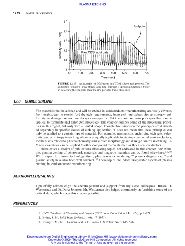
1.5
Endpoint
1.4
Intensity (arb. units) 1.3 Raw OES input data
1.2
1.1
1
0 100 200 300 400 500 600 700
Time (sec)
FIGURE 12.17 An example of OES traces in a TDM silicon etch process. The
converted “envelop” trace (thick solid line) through a special algorithm is better
in detecting the endpoint than the raw periodic trace (thin line).
12.6 CONCLUSIONS
The materials that have been and will be etched in semiconductor manufacturing are vastly diverse,
from mainstream to exotic. And the etch requirements, from etch rate, selectivity, anisotropy, uni-
formity to damage control, are always case-specific. Yet there are common principles that can be
applied to formulate and tailor etch processes. This chapter outlines some of the processing princi-
ples in this regard, but only with a limited scope. Though discussions on the principles are illustrat-
ed separately in specific classes of etching application, it does not mean that these principles can
only be applied to a certain type of material. For example, mechanisms underlying etch rate, selec-
tivity, and anisotropy in etching silicon are equally applicable to etching compound semiconductors;
mechanisms related to plasma chemistry and surface morphology and damage control in etching III-
V semiconductor can be applied to other compound materials such as II-VI semiconductors.
There exists a wealth of publications discussing topics not addressed in this chapter. For exam-
ple, plasma etching of photomask materials and magnetic materials can be found elsewhere. 103,104
With respect to plasma technology itself, plasma reactor modeling, 105 plasma diagnostics, 106 and
plasma safety have also been well covered. 107 These topics are indeed inseparable aspects of plasma
etching in semiconductor manufacturing.
ACKNOWLEDGMENTS
I gratefully acknowledge the encouragement and support from my close colleagues—Russell J.
Westerman and Dr. Dave Johnson. Mr. Westerman also helped enormously in furnishing some of the
critical data, which made this chapter possible.
REFERENCES
1. CRC Handbook of Chemistry and Physics (CRC Press, Boca Raton, FL, 1979), p. F-121.
2. Irving, S. M., Solid State Technol., 14(6), 47 (1971).
3. Irving, S. M., K. E. Lemons, and G. E. Bobos, U.S. Patent No. 3, 615, 596.
Downloaded from Digital Engineering Library @ McGraw-Hill (www.digitalengineeringlibrary.com)
Copyright © 2004 The McGraw-Hill Companies. All rights reserved.
Any use is subject to the Terms of Use as given at the website.