
Page 1094 - The Mechatronics Handbook
P. 1094
+ P N
- i
ANODE CATHODE
Forward Bias Direction
FIGURE 40.4 The diode and its behavior.
C
N P N
EMITTER COLLECTOR B NPN
BASE
(a) E
C
P N P B
EMITTER COLLECTOR PNP
BASE E
(b)
FIGURE 40.5 (a) npn-transistor symbol, (b) pnp-transistor symbol.
V
3 LEADS CC
E B C i
C
i C +
B
V B
BB ν
+ CE
-
ν E
BE
i
E
-
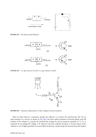
FIGURE 40.6 Schematic representation of the working of an npn-transistor.
There are three leads in a transistor, namely, the collector (C), emitter (E), and the base (B). For an
npn-transistor in a circuit, as shown in Fig. 40.6, the base–emitter junction is forward biased and will
conduct if the voltage V BE exceeds the forward bias voltage for the pn-junction, typically 0.7 V. V BE is
increased by increasing the voltage at B. However, the base–collector junction is reverse biased as the
collector C is at a higher potential. As current flows in the base–emitter loop, the electrons from the emitter
©2002 CRC Press LLC