
Page 1095 - The Mechatronics Handbook
P. 1095
D
S G D
G
N N
P N - MOSFET
S
D
S G D
G
P P
N P - MOSFET
S
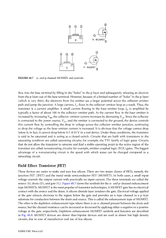
FIGURE 40.7 n- and p-channel MOSFETs and symbols.
flow into the base terminal by filling in the “holes” in the p-layer and subsequently releasing an electron
from the p-layer out of the base terminal. However, because of a limited number of “holes” in the p-layer
(which is very thin), the electrons from the emitter see a larger potential across the collector–emitter
path and jump the junction. A large current, I C , flows in the collector–emitter loop as a result. Thus, the
transistor is a current amplifier. A small current flowing in the base–emitter loop, I B , is amplified by
typically a factor of about 100 in the collector–emitter path. As the current flow in the base–emitter is
increased by increasing V BE , the collector–emitter current increases by decreasing V CE . Since the collector
is connected to the power source, V CC , and the emitter is connected to the ground, the device controls
this current flow by controlling the drop in voltage across the collector–emitter junction, continuing
to drop the voltage as the base–emitter current is increased. It is obvious that the voltage cannot drop
below 0; in fact, it cannot drop below 0.2–0.35 V in a real device. Under these conditions, the transistor
is said to be saturated and is acting as a closed switch. Circuits that are built with transistors in the
saturating condition are called saturating circuits; for example, the TTL family of logic gates. Circuits
that do not allow the transistor to saturate and find a stable operating point in the active region of the
transistor are called nonsaturating circuits; for example, emitter-coupled logic (ECL) gates. The biggest
advantage of a nonsaturating circuit is the speed with which states can be changed compared to a
saturating circuit.
Field Effect Transistor (FET)
These devices are easier to make and uses less silicon. There are two major classes of FETs, namely, the
junction FET (JFET) and the metal oxide semiconductor FET (MOSFET). In both cases, a small input
voltage controls the output current with practically no input current. The three terminals are called the
source (S), drain (D), and gate (G). Figure 40.7 shows the symbols for the n- and p-channel enhancement
type MOSFETs. MOSFET is the most popular of transistor technologies. A MOSFET gate has no electrical
contact with the source and the drain. A silicon-dioxide layer insulates the gate. Electrical voltage applied
at the gate attracts electrons to the region below the gate and provides an n-type channel in a p-type
substrate for conduction between the drain and source. This is called the enhancement type of MOSFET.
The other is the depletion-enhancement type where there is an n-channel present between the drain and
source, but the channel resistance can be increased or decreased by applying either a negative or a positive
voltage at the gate, respectively. Depletion-enhancement MOSFET symbols and function are described
in Fig. 40.8. MOSFET devices are slower than bipolar devices and are used in slower but high density
circuits, due to ease of manufacture and use of less silicon.
©2002 CRC Press LLC