
Page 1100 - The Mechatronics Handbook
P. 1100
0066_Frame_C40 Page 10 Wednesday, January 9, 2002 8:21 PM
t r t f
(V H ) 100%
90%
V IH(min)
V T
t w
V IL(max)
10%
(V L ) 0%
Time
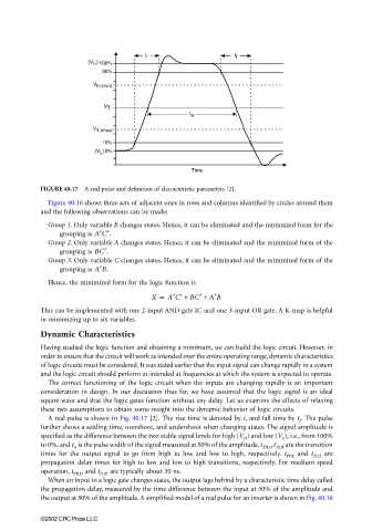
FIGURE 40.17 A real pulse and definition of characteristic parameters [2].
Figure 40.16 shows three sets of adjacent ones in rows and columns identified by circles around them
and the following observations can be made:
Group 1. Only variable B changes states. Hence, it can be eliminated and the minimized form for the
grouping is A′C′ .
Group 2. Only variable A changes states. Hence, it can be eliminated and the minimized form of the
grouping is BC′ .
Group 3. Only variable C changes states. Hence, it can be eliminated and the minimized form of the
grouping is A′B .
Hence, the minimized form for the logic function is
X = A′C′ + BC′ + A′B
This can be implemented with one 2-input AND gate IC and one 3-input OR gate. A K-map is helpful
in minimizing up to six variables.
Dynamic Characteristics
Having studied the logic function and obtaining a minimum, we can build the logic circuit. However, in
order to ensure that the circuit will work as intended over the entire operating range, dynamic characteristics
of logic circuits must be considered. It was stated earlier that the input signal can change rapidly in a system
and the logic circuit should perform as intended at frequencies at which the system is expected to operate.
The correct functioning of the logic circuit when the inputs are changing rapidly is an important
consideration in design. In our discussion thus far, we have assumed that the logic signal is an ideal
square wave and that the logic gates function without any delay. Let us examine the effects of relaxing
these two assumptions to obtain some insight into the dynamic behavior of logic circuits.
A real pulse is shown in Fig. 40.17 [2]. The rise time is denoted by t r and fall time by t f . The pulse
further shows a settling time, overshoot, and undershoot when changing states. The signal amplitude is
specified as the difference between the two stable signal levels for high (V H ) and low (V L ), i.e., from 100%
to 0%, and t w is the pulse width of the signal measured at 50% of the amplitude. t THL , t TLH are the transition
times for the output signal to go from high to low and low to high, respectively. t PHL and t PLH are
propagation delay times for high to low and low to high transitions, respectively. For medium speed
operation, t PHL , and t PLH are typically about 30 ns.
When an input to a logic gate changes states, the output lags behind by a characteristic time delay called
the propagation delay, measured by the time difference between the input at 50% of the amplitude and
the output at 50% of the amplitude. A simplified model of a real pulse for an inverter is shown in Fig. 40.18
©2002 CRC Press LLC