
Page 1102 - The Mechatronics Handbook
P. 1102
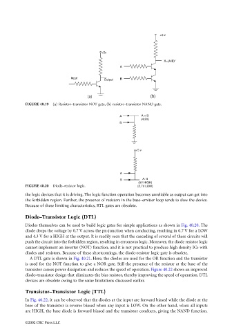
+5 v


                                                                   +5v
                                                                                              X=(A.B)'
                                                                           A

                                                     Input                 B
                                                                    Output


                                                            (a)                         (b)
                                 FIGURE 40.19  (a) Resistor–transistor NOT gate, (b) resistor–transistor NAND gate.

                                                                          A         A + B
                                                                                    (4.3V)
                                                                          B


                                                                                 +5 v


                                                                           A
                                                                           B        A. B
                                                                                   (5V HIGH)
                                 FIGURE 40.20  Diode–resistor logic.              (0.7V LOW)
                                 the logic devices that it is driving. The logic function operation becomes unreliable as output can get into
                                 the forbidden region. Further, the presence of resistors in the base–emitter loop tends to slow the device.
                                 Because of these limiting characteristics, RTL gates are obsolete.

                                 Diode–Transistor Logic (DTL)
                                 Diodes themselves can be used to build logic gates for simple applications as shown in Fig. 40.20. The
                                 diode drops the voltage by 0.7 V across the pn-junction when conducting, resulting in 0.7 V for a LOW
                                 and 4.3 V for a HIGH at the output. It is readily seen that the cascading of several of these circuits will
                                 push the circuit into the forbidden region, resulting in erroneous logic. Moreover, the diode resistor logic
                                 cannot implement an inverter (NOT) function, and it is not practical to produce high density ICs with
                                 diodes and resistors. Because of these shortcomings, the diode-resistor logic gate is obsolete.
                                   A DTL gate is shown in Fig. 40.21. Here, the diodes are used for the OR function and the transistor
                                 is used for the NOT function to give a NOR gate. Still the presence of the resistor at the base of the
                                 transistor causes power dissipation and reduces the speed of operation. Figure 40.22 shows an improved
                                 diode–transistor design that eliminates the bias resistor, thereby improving the speed of operation. DTL
                                 devices are obsolete owing to the same limitations discussed earlier.
                                 Transistor–Transistor Logic (TTL)

                                 In Fig. 40.22, it can be observed that the diodes at the input are forward biased while the diode at the
                                 base of the transistor is reverse biased when any input is LOW. On the other hand, when all inputs
                                 are HIGH, the base diode is forward biased and the transistor conducts, giving the NAND function.

                                 ©2002 CRC Press LLC