
Page 1104 - The Mechatronics Handbook
P. 1104
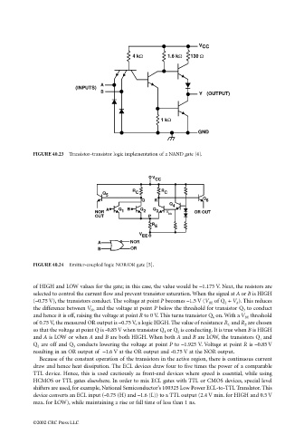
V CC
                                                                  4 kΩ        1.6 kΩ  130 Ω


                                                        A
                                               (INPUTS)
                                                        B
                                                                                        Y (OUTPUT)


                                                                            1 kΩ

                                                                                        GND


                                 FIGURE 40.23  Transistor–transistor logic implementation of a NAND gate [4].


                                                                         V
                                                                          CC
                                                                  R         R
                                                        Q          C         C
                                                         5
                                                                                          Q
                                                                     Q    R                6
                                                                               Q 4
                                                          A   Q  B   Q   Q
                                                      NOR      1      2   3  V         OR OUT
                                                      OUT               P     bb
                                                                         R
                                                                          E
                                                                     V
                                                                      EE
                                                       A          NOR
                                                       B          OR
                                 FIGURE 40.24  Emitter-coupled logic NOR/OR gate [5].


                                 of HIGH and LOW values for the gate; in this case, the value would be –1.175 V. Next, the resistors are
                                 selected to control the current flow and prevent transistor saturation. When the signal at A or B is HIGH
                                 (–0.75 V), the transistors conduct. The voltage at point P becomes –1.5 V (V BE  of Q 2  + V A ). This reduces
                                 the difference between V bb  and the voltage at point P below the threshold for transistor Q 3  to conduct
                                 and hence it is off, raising the voltage at point R to 0 V. This turns transistor Q 6  on. With a V BE  threshold
                                 of 0.75 V, the measured OR output is –0.75 V, a logic HIGH. The value of resistance R C  and R E  are chosen
                                 so that the voltage at point Q is -0.85 V when transistor Q 1  or Q 2  is conducting. It is true when B is HIGH
                                 and A is LOW or when A and B are both HIGH. When both A and B are LOW, the transistors Q 1  and
                                 Q 2  are off and Q 3  conducts lowering the voltage at point P to –1.925 V. Voltage at point R is –0.85 V
                                 resulting in an OR output of  –1.6 V at the OR output and -0.75 V at the NOR output.
                                   Because of the constant operation of the transistors in the active region, there is continuous current
                                 draw and hence heat dissipation. The ECL devices draw four to five times the power of a comparable
                                 TTL device. Hence, this is used cautiously as front-end devices where speed is essential, while using
                                 HCMOS or TTL gates elsewhere. In order to mix ECL gates with TTL or CMOS devices, special level
                                 shifters are used, for example, National Semiconductor’s 100325 Low Power ECL-to-TTL Translator. This
                                 device converts an ECL input (-0.75 (H) and –1.6 (L)) to a TTL output (2.4 V min. for HIGH and 0.5 V
                                 max. for LOW), while maintaining a rise or fall time of less than 1 ns.


                                 ©2002 CRC Press LLC