
Page 1105 - The Mechatronics Handbook
P. 1105
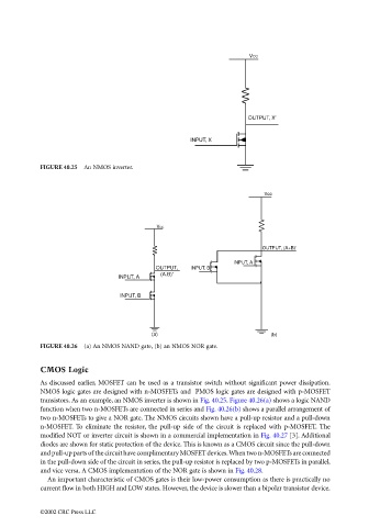
VCC


                                                                                          OUTPUT, X'


                                                                          INPUT, X


                                 FIGURE 40.25  An NMOS inverter.


                                                                                               Vcc


                                                                 VCC

                                                                                              OUTPUT, (A+B)'
                                                                                      INPUT, A
                                                                 OUTPUT,   INPUT, B
                                                                  (A.B)'
                                                       INPUT, A

                                                       INPUT, B


                                                                (a)                             (b)
                                 FIGURE 40.26  (a) An NMOS NAND gate, (b) an NMOS NOR gate.

                                 CMOS Logic

                                 As discussed earlier, MOSFET can be used as a transistor switch without significant power dissipation.
                                 NMOS logic gates are designed with n-MOSFETs and  PMOS logic gates are designed with p-MOSFET
                                 transistors. As an example, an NMOS inverter is shown in Fig. 40.25. Figure 40.26(a) shows a logic NAND
                                 function when two n-MOSFETs are connected in series and Fig. 40.26(b) shows a parallel arrangement of
                                 two n-MOSFETs to give a NOR gate. The NMOS circuits shown have a pull-up resistor and a pull-down
                                 n-MOSFET. To eliminate the resistor, the pull-up side of the circuit is replaced with p-MOSFET. The
                                 modified NOT or inverter circuit is shown in a commercial implementation in Fig. 40.27 [3]. Additional
                                 diodes are shown for static protection of the device. This is known as a CMOS circuit since the pull-down
                                 and pull-up parts of the circuit have complimentary MOSFET devices. When two n-MOSFETs are connected
                                 in the pull-down side of the circuit in series, the pull-up resistor is replaced by two p-MOSFETs in parallel,
                                 and vice versa. A CMOS implementation of the NOR gate is shown in Fig. 40.28.
                                   An important characteristic of CMOS gates is their low-power consumption as there is practically no
                                 current flow in both HIGH and LOW states. However, the device is slower than a bipolar transistor device.


                                 ©2002 CRC Press LLC