
Page 1101 - The Mechatronics Handbook
P. 1101
t r t f
V DD
90%
INPUT 50%
10%
t THL t TLH
V DD
90%
50%
INVERTING
OUTPUT 10%
t PHL t PLH
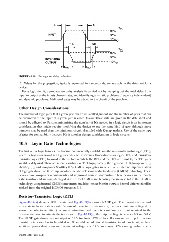
FIGURE 40.18 Propagation delay definition.
[3]. Values for the propagation, typically expressed in nanoseconds, are available in the datasheet for a
device.
For a logic circuit, a propagation delay analysis is carried out by mapping out the total delay from
input to output as the inputs change states, and identifying any static problems (frequency independent)
and dynamic problems. Additional gates may be added to the circuit of the problem.
Other Design Considerations
The number of logic gates that a given gate can drive is called fan-out and the number of gates that can
be connected to the input of a given gate is called fan-in. These data are given in the data sheet and
should be adhered to. Further, minimizing the number of ICs needed in a logic circuit is an important
consideration that might require modifying the design to use the same kind of gate although more
numbers may be used than the minimum circuit identified with K-map analysis. Use of the same type
of gates for compatibility between ICs is another design consideration in logic circuits.
40.5 Logic Gate Technologies
The first of the logic families that became commercially available was the resistor–transistor logic (RTL),
where the transistor is used as a high-speed switch in circuits. Diode–transistor logic (DTL) and transistor–
transistor logic (TTL) followed in the evolution. While the RTL and the DTL are obsolete, the TTL gates
are still widely used. There are several variations of TTL logic, namely, the high-speed (H), low-power (L),
Shottkey (S), and low-power Shottkey (LS). CMOS logic gates are an entirely different implementation
of logic gates based on the complimentary metal-oxide semiconductor devices (CMOS) technology. These
devices have low-power requirements and improved noise characteristics. These devices are extremely
static sensitive and are easily damaged. A mixture of CMOS and bipolar processes resulted in the BiCMOS
technology, using internal CMOS components and high-power bipolar outputs. Several different families
evolved from the original BiCMOS processes [1].
Resistor–Transistor Logic (RTL)
Figure 40.19(a) shows an RTL inverter and Fig. 40.19(b) shows a NAND gate. The transistor is assumed
to operate in the saturation mode. Because of the nature of a transistor, there is a minimum voltage drop
across the collector–emitter junction at saturation and there is a minimum current required in the
base–emitter loop to saturate the transistor. In Fig. 40.19(a), the output voltage is between 0.3 and 5.0 V.
The NAND gate shown has an output of 0.6 V for logic LOW as the collector–emitter drop for the two
transistors in series has to be added up. If we add an additional transistor to add an input, we have
additional power dissipation and the output voltage is at 0.9 V for a logic LOW causing problems with
©2002 CRC Press LLC