Page 1106 - The Mechatronics Handbook
P. 1106

V DD
                                                                            V DD


                                                                                          _
                                                                                        G=A
                                                                                         G
                                                      A
                                                      INPUT                             OUTPUT


                                                                                   V SS


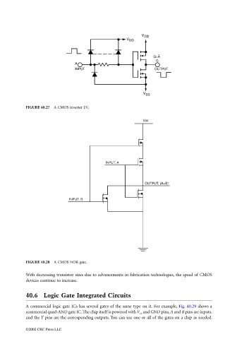
                                 FIGURE 40.27  A CMOS inverter [3].


                                                                                   Vcc


                                                                   INPUT, A


                                                                                    OUTPUT, (A+B)'


                                                    INPUT, B


                                 FIGURE 40.28  A CMOS NOR gate.

                                 With decreasing transistor sizes due to advancements in fabrication technologies, the speed of CMOS
                                 devices continue to increase.


                                 40.6 Logic Gate Integrated Circuits

                                 A commercial logic gate ICs has several gates of the same type on it. For example, Fig. 40.29 shows a
                                 commercial quad-AND gate IC. The chip itself is powered with V cc  and GND pins, A and B pins are inputs,
                                 and the Y pins are the corresponding outputs. You can use one or all of the gates on a chip as needed.

                                 ©2002 CRC Press LLC
   1101   1102   1103   1104   1105   1106   1107   1108   1109   1110   1111