
Page 1107 - The Mechatronics Handbook
P. 1107
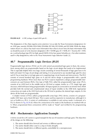
1A
                                                                                      1Y
                                                                         1B
                                                                        2A
                                                                                      2Y
                                                                         2B
                                                                         3A
                                                           1A  1  14 Vcc  3B          3Y
                                                           1B  2  13 4B
                                                           1Y  3  12 4A  4A
                                                           2A  4  11 4Y                4Y
                                                           2B  5  10 3B  4B
                                                           2Y  6  9 3A
                                                         GND  7  8 3Y        Y = A . B

                                 FIGURE 40.29   A DIP package of quad-AND gate IC.

                                 The designation of the chips requires some attention. Let us take the Texas Instruments designations for
                                 an AND gate, namely, SN5408, SN54LS08, SN54S08, SN7408, SN74LS08, and SN74S08. While the desig-
                                 nation shown on a device has much more information than what is shown here, the basic information that
                                 we should be aware of is the function designation (00 = NAND gate, 02 = NOR, 04 = Inverter, 08 = AND,
                                 etc.), and technology type (HC for high-speed CMOS, LS for low-power Schottky, etc.). For other notations
                                 used in chip designations, refer to the Texas Instruments Logic Selection Guide [1].


                                 40.7 Programmable Logic Devices (PLD)

                                 Programmable logic devices (PLDs) are ICs with several uncommitted logic gates in them, the connec-
                                 tions among which are programmable based on the logic circuit design that needs to be implemented.
                                 This is especially helpful when very large circuits consisting of several thousands of logic gates have to be
                                 built and tested. For large circuit design and testing, it is not practical to use standard logic gate ICs since
                                 each IC has at most four or six logic gates on it, requiring large circuit boards and interconnects. The PLD
                                 consists of several hundred logic gates on it and the device design is programmable with a special
                                 programming hardware. When more than one PLD is used to implement a design, programmable inter-
                                 connects are used between PLDs. One type of fully PLD, called  the  programmable  logic  array  (PLA),
                                 consists of an AND level in the middle and an OR level at output, similar to a TTL single logic gate
                                 structure, with both layers being programmable. All input signals are connected to an inverter level, which
                                 provides both the normal and complemented values of input variables to the AND level. Appropriate
                                 connections are made at the AND level and at the OR level to produce the desired logic outputs. In this
                                 device all the levels are programmable.
                                   A simpler version of PLD, called a programmable array logic (PAL) device, consists of a program-
                                 mable AND layer and a fixed OR layer. This is easier and less expensive to manufacture, although it is
                                 not as flexible as a PLA. A variety of combinations is available to suit various needs. A schematic of a
                                 PLA is shown in Fig. 40.30 [6] where the connections to be made in the hardware are marked with an
                                 X. When programmed these connections will be made or “fused” and verified by the programming
                                 hardware.


                                 40.8 Mechatronics Application Example

                                 A driver circuit for a DC motor is a good example for the use of transistors and logic gates. The objectives
                                 of the design are the following:

                                    1. The motor should drive forward and reverse at different speeds.
                                    2. The motor should either coast to a stop or brake abruptly.
                                    3.  The motor should drive at different speeds, controllable by a microprocessor.

                                 ©2002 CRC Press LLC