
Page 519 - The Mechatronics Handbook
P. 519
0066_frame_C19 Page 141 Wednesday, January 9, 2002 5:32 PM
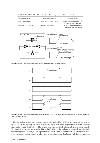
TABLE 19.7 A List of Possible Materials for Diaphragm and the Piezoresistive Sensors
Diaphragm material Piezoresistor material Relative merits
Single crystal silicon Doped single crystal silicon Relatively difficult to control the
thickness of the diaphragm
Silicon nitride thin film Polycrystalline silicon Easy to form thin diaphragms;
involved LPCVD polysilicon
FIGURE 19.113 Schematic diagram of a bulk micromachined pressure sensor.
FIGURE 19.114 Schematic diagram illustrating major steps in the microfabrication process of a bulk microma-
chined pressure sensor.
The fabrication process for a pressure sensor using plain silicon wafer as the substrate is shown in
Fig. 19.114. In the first step, the wafer is selectively doped with boron or phosphorous atoms to create
piezoresistors on the front side (a). The wafer is then passivated with a thermally grown silicon dioxide
thin film (b). In the ensuing step, the silicon dioxide film on the backside is patterned and selectively
etched to expose the silicon (c). The exposed silicon material will be etched when the wafer is immersed
in an anisotropic silicon etchant (d). In order to form the silicon diaphragm with desired thickness,
©2002 CRC Press LLC