
Page 521 - The Mechatronics Handbook
P. 521
0066_frame_C19 Page 143 Wednesday, January 9, 2002 5:32 PM
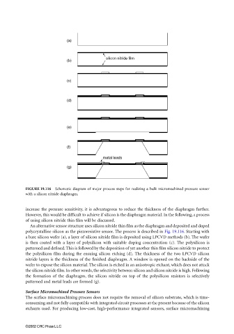
FIGURE 19.116 Schematic diagram of major process steps for realizing a bulk micromachined pressure sensor
with a silicon nitride diaphragm.
increase the pressure sensitivity, it is advantageous to reduce the thickness of the diaphragm further.
However, this would be difficult to achieve if silicon is the diaphragm material. In the following, a process
of using silicon nitride thin film will be discussed.
An alternative sensor structure uses silicon nitride thin film as the diaphragm and deposited and doped
polycrystalline silicon as the piezoresistive sensor. The process is described in Fig. 19.116. Starting with
a bare silicon wafer (a), a layer of silicon nitride film is deposited using LPCVD methods (b). The wafer
is then coated with a layer of polysilicon with suitable doping concentration (c). The polysilicon is
patterned and defined. This is followed by the deposition of yet another thin film silicon nitride to protect
the polysilicon film during the ensuing silicon etching (d). The thickness of the two LPCVD silicon
nitride layers is the thickness of the finished diaphragm. A window is opened on the backside of the
wafer to expose the silicon material. The silicon is etched in an anisotropic etchant, which does not attack
the silicon nitride film. In other words, the selectivity between silicon and silicon nitride is high. Following
the formation of the diaphragm, the silicon nitride on top of the polysilicon resistors is selectively
patterned and metal leads are formed (g).
Surface Micromachined Pressure Sensors
The surface micromachining process does not require the removal of silicon substrate, which is time-
consuming and not fully compatible with integrated circuit processes at the present because of the silicon
etchants used. For producing low-cost, high-performance integrated sensors, surface micromachining
©2002 CRC Press LLC