
Page 520 - The Mechatronics Handbook
P. 520
0066_frame_C19 Page 142 Wednesday, January 9, 2002 5:32 PM
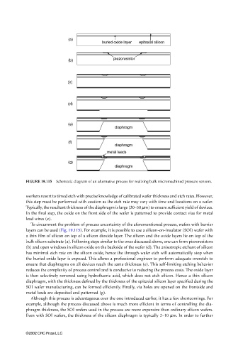
FIGURE 19.115 Schematic diagram of an alternative process for realizing bulk micromachined pressure sensors.
workers resort to timed etch with precise knowledge of calibrated wafer thickness and etch rates. However,
this step must be performed with caution as the etch rate may vary with time and locations on a wafer.
Typically, the resultant thickness of the diaphragm is large (30–50 µm) to ensure sufficient yield of devices.
In the final step, the oxide on the front side of the wafer is patterned to provide contact vias for metal
lead wires (e).
To circumvent the problem of process uncertainty of the aforementioned process, wafers with barrier
layers can be used (Fig. 19.115). For example, it is possible to use a silicon-on-insulator (SOI) wafer with
a thin film of silicon on top of a silicon dioxide layer. The silicon and the oxide layers lie on top of the
bulk silicon substrate (a). Following steps similar to the ones discussed above, one can form piezoresistors
(b) and open windows in silicon oxide on the backside of the wafer (d). The anisotropic etchant of silicon
has minimal etch rate on the silicon oxide, hence the through-wafer etch will automatically stop when
the buried oxide layer is exposed. This allows a professional engineer to perform adequate overetch to
ensure that diaphragms on all devices reach the same thickness (e). This self-limiting etching behavior
reduces the complexity of process control and is conducive to reducing the process costs. The oxide layer
is then selectively removed using hydrofluoric acid, which does not etch silicon. Hence a thin silicon
diaphragm, with the thickness defined by the thickness of the epitaxial silicon layer specified during the
SOI wafer manufacturing, can be formed efficiently. Finally, via holes are opened on the frontside and
metal leads are deposited and patterned (g).
Although this process is advantageous over the one introduced earlier, it has a few shortcomings. For
example, although the process discussed above is much more efficient in terms of controlling the dia-
phragm thickness, the SOI wafers used in the process are more expensive than ordinary silicon wafers.
Even with SOI wafers, the thickness of the silicon diaphragm is typically 2–10 µm. In order to further
©2002 CRC Press LLC