
Page 524 - The Mechatronics Handbook
P. 524
0066_frame_C19 Page 146 Wednesday, January 9, 2002 5:32 PM
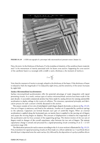
FIGURE 19.119 A SEM micrograph of a prototype bulk micromachined pressure sensor (Junjun Li).
Here, the term t is the thickness of the beam, E is the modulus of elasticity of the cantilever beam material,
and I is the momentum of inertia associated with the beam cross section. Supposing the cross section
of the cantilever beam is a rectangle with a width w and a thickness t, the moment of inertia is
I = wt 3
--------
12
Note that the moment of inertia is strongly related to the thickness of the beam. If the thickness of beam
is reduced to half, the magnitude of I is reduced by eight times, and the sensitivity of the sensor increases
by eight fold.
Surface Micromachined Accelerometers
Surface micromachined accelerometers offer the potential advantage of ready integration with signal
processing circuits. As a result, various types of surface micromachined versions have been made in the
past decade. A successful commercial product has been made by analog devices for sensing automobile
acceleration to deploy airbags in the events of collision. The structure, operational principle, and fabri-
cation process for such a sensor is briefly discussed in this section.
The sensor consists of two sets of interdigited comb-finger-shaped electrodes as shown in Fig. 19.120.
One set of fingers is stationary and fixed to the substrate. Another set if suspended by cantilever springs
to the substrate. Capacitors are formed between each pair of comb-like fingers. When an external
acceleration is applied along the horizontal axis, an inertia force is applied to the moving set of fingers
and causes the moving fingers to displace. The amount of displacement is related to the magnitude of
the acceleration and the force constant of the supporting springs. The relative motion of the two sets of
fingers result in changes of the overall capacitance value between the two sets of fingers. The minute
capacitance change is sensed and processed by a signal-processing circuit consisting of an Σ − ∆ A/D
conversion stage [10].
The fabrication process for such a sensor according to the A-A cross-section is illustrated in Fig. 19.121.
First, transistors for signal processing circuits are first made on a silicon substrate (a). A sacrificial silicon
dioxide layer is deposited onto the wafer surface (b), followed by the deposition of a polycrystalline silicon
©2002 CRC Press LLC