
Page 525 - The Mechatronics Handbook
P. 525
0066_frame_C19 Page 147 Wednesday, January 9, 2002 5:32 PM
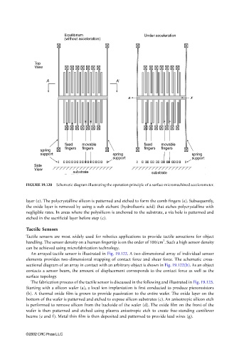
FIGURE 19.120 Schematic diagram illustrating the operation principle of a surface micromachined accelerometer.
layer (c). The polycrystalline silicon is patterned and etched to form the comb fingers (e). Subsequently,
the oxide layer is removed by using a web etchant (hydrofluoric acid) that etches polycrystalline with
negligible rates. In areas where the polysilicon is anchored to the substrate, a via hole is patterned and
etched in the sacrificial layer before step (c).
Tactile Sensors
Tactile sensors are most widely used for robotics applications to provide tactile sensations for object
2
handling. The sensor density on a human fingertip is on the order of 100/cm . Such a high sensor density
can be achieved using microfabrication technology.
An arrayed tactile sensor is illustrated in Fig. 19.122. A two-dimensional array of individual sensor
elements provides two-dimensional mapping of contact force and shear force. The schematic cross-
sectional diagram of an array in contact with an arbitrary object is shown in Fig. 19.122(b). As an object
contacts a sensor beam, the amount of displacement corresponds to the contact force as well as the
surface topology.
The fabrication process of the tactile sensor is discussed in the following and illustrated in Fig. 19.123.
Starting with a silicon wafer (a), a local ion implantation is first conducted to produce piezoresistors
(b). A thermal oxide film is grown to provide passivation to the entire wafer. The oxide layer on the
bottom of the wafer is patterned and etched to expose silicon substrates (c). An anisotropic silicon etch
is performed to remove silicon from the backside of the wafer (d). The oxide film on the front of the
wafer is then patterned and etched using plasma anisotropic etch to create free-standing cantilever
beams (e and f). Metal thin film is then deposited and patterned to provide lead wires (g).
©2002 CRC Press LLC