
Page 522 - The Mechatronics Handbook
P. 522
0066_frame_C19 Page 144 Wednesday, January 9, 2002 5:32 PM
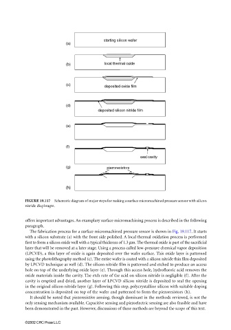
FIGURE 19.117 Schematic diagram of major steps for making a surface micromachined pressure sensor with silicon
nitride diaphragm.
offers important advantages. An examplary surface micromachining process is described in the following
paragraph.
The fabrication process for a surface micromachined pressure sensor is shown in Fig. 19.117. It starts
with a silicon substrate (a) with the front side polished. A local thermal oxidation process is performed
first to form a silicon oxide well with a typical thickenss of 1.3 µm. The thermal oxide is part of the sacrificial
layer that will be removed at a later stage. Using a process called low-pressure chemical vapor deposition
(LPCVD), a thin layer of oxide is again deposited over the wafer surface. This oxide layer is patterned
using the photolithography method (c). The entire wafer is coated with a silicon nitride thin film deposited
by LPCVD technique as well (d). The silicon nitride film is patterned and etched to produce an access
hole on top of the underlying oxide layer (e). Through this access hole, hydrofluoric acid removes the
oxide materials inside the cavity. The etch rate of the acid on silicon nitride is negligible (f). After the
cavity is emptied and dried, another layer of LPCVD silicon nitride is deposited to seal the opening
in the original silicon nitride layer (g). Following this step, polycrystalline silicon with suitable doping
concentration is deposited on top of the wafer and patterned to form the piezoresistors (h).
It should be noted that piezoresistive sensing, though dominant in the methods reviewed, is not the
only sensing mechanism available. Capacitive sensing and piezoelectric sensing are also feasible and have
been demonstrated in the past. However, discussions of these methods are beyond the scope of this text.
©2002 CRC Press LLC