
Page 640 - The Mechatronics Handbook
P. 640
0066_Frame_C20.fm Page 110 Wednesday, January 9, 2002 1:46 PM
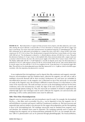
1 UV light
Photolithography Mask
Photoresist
Silicon Substrate
2 Development
Silicon Substrate
3 Copper Electrodeposition
Electrodeposited Cu
Silicon Substrate
4 Removal and Etching
Electrodeposited Cu
Silicon Substrate
FIGURE 20.131 Electrodeposition of copper and basic processes: silicon, kapton, and other substrates, can be used.
After clearing, the silicon substrate is covered with a 5–10 nm chromium or titanium and 100–200 nm copper seed
layer by sputtering. The copper microcoils (microstructures) are patterned using the UV photolitography. The AZ-
4562 photoresist can be spincoated and prebaked on a ramped hot plate at 90–100°C (ramp 30–40% with initial
temperature 20–25°C) for one hour. Then, the photoresist is exposed in the Karl Suss Contact Masker with the energy
2
1200–1800 mJ cm . The development is released in 1:4 diluted alkaline solution (AZ-400) for 4–6 min. This gives
the photoresist thickness 15–25 µm. Copper is electroplated with a three-electrode system with a copper anode and
a saturated calomel reference electrode (the current power supply is the Perkin Elmer Current Source EG&G 263).
The Shipley sulfate bath with the 5–10 ml/l brightener to smooth the deposit can be used. The electrodeposition is
2
performed at 20–25°C with magnetic stirring and the dc current density 40–60 mA/cm (this current density leads
to smooth copper thin films with the 5–10 nm rms roughness for the 10 mm thickness of the deposited copper thin
film). The resistivity of the electrodeposited copper thin film (microcoils) is 1.6–1.8 µΩ cm (close to the bulk copper
resistivity). After the deposition, the photoresist is removed.
It was emphasized that electroplating is used to deposit thin-film conductors and magnetic materials.
However, microtransducers need the insulation layers, otherwise the magnetic core and coils as well as
multilayer microcoils themself will be short-circuited. Furthermore, the seed layers are embedded in
microfabrication processes. As the magnetic core is fabricated on top of the microcoils (or microcoils
are made on the magnetic core), the seed layer is difficult to remove because it is at the bottom or at the
center of the microstructure. The mesh seed layer can serve as the electroplating seed layer for the lower
conductors, and as the microstructure is made, the edges of the mesh seed layer can be exposed and
removed through plasma etching [6]. Thus, the microcoils are insulated. It should be emphasized that
relatively high aspect ratio techniques must be used to fabricate the magnetic core and microcoils, and
patterning as well as surface planarization issues must be addressed.
NiFe Thin Films Electrodeposition
Magnetic cores in microstructures and microtransducers must be made. For example, the electroplated
Ni x% Fe 100−x% thin films, such as permalloy Ni 80% Fe 20% , can be deposited to form the magnetic core of
microtransducers (actuators and sensors), inductors, transformers, switches, etc. The basic processes and
sequential steps used are similar to the processes for the copper electrodeposition and the electroplating
is done in the electroplating bath. The windings (microcoils) must be insulated from magnetic cores,
and therefore, the insulation layers must be deposited. The insulating materials used to insulate the
windings from the magnetic core are benzocyclobutene, polyimide (PI-2611), etc. For example, the cyclo-
tene 7200-35 is photosensitive and can be patterned through photolithography. The benzocyclobutene,
©2002 CRC Press LLC