Page 639 - The Mechatronics Handbook
P. 639
0066_Frame_C20.fm  Page 109  Wednesday, January 9, 2002  1:46 PM


                       materials, and sequential steps are different depending on the MEMS which must be devised, designed,
                       analyzed, and optimized first.

                       Conductor Thin Films Electrodeposition
                       The conductors (microcoils to make windings) in microstructures and microtransducers can be fabricated
                       by electrodepositing the copper and other low resistivity metals. Electrodeposition of metals is made by
                       immersing a conductive surface in a solution containing ions of the metal to be deposited. The surface
                       is electrically connected to an external power supply, and current is fed through the surface into the
                                                                  x+               −
                       solution. In general, the reaction of the metal ions (Metal ) with x electrons (xe ) to form metal (Metal)
                             x+   −
                       is Metal  + xe  = Metal.
                         To electrodeposit copper on the silicon wafer, the wafer is typically coated with a thin conductive
                       layer of copper (seed layer) and immersed in a solution containing cupric ions. Electrical contact is
                                                                                    2+   −
                       made to the seed layer, and current is flowed (passed) such that the reaction Cu  + 2e  → Cu occurs at
                       the wafer surface. The wafer, which is electrically interacted such that the metal ions are changed to
                       metal atoms, is the cathode. Another electrically active surface (anode) is the conductive solution to
                       make the electrical path. At the anode, the oxidation reaction occurs that balances the current flow at
                       the cathode, thus maintaining the electric neutrality. In the case of copper electroplating, all cupric ions
                       removed from solution at the wafer cathode are replaced by dissolution from the copper anode.
                       According to the Faraday law of electrolysis, in the absence of secondary reactions, the current delivered
                       to a conductive surface during electroplating is proportional to the quantity of the metal deposited.
                       Thus, the metal deposited can be controlled varying the electroplating current (current density) and
                       the electrodeposition time.
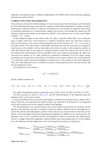
                         The hydrated Cu ions reaction is

                                                        ++
                                                               (
                                                      Cu →   Cu H 2 O) ++
                                                                     6
                       and the cathode reactions are


                                          ++
                               −
                                                    +
                                              −
                                                                                 ++
                                                                                           +
                                                                                              −
                                                          +
                                                              −
                                                                          +
                         ++
                       Cu +  2e →  Cu,  Cu + e →  Cu ,  Cu +  e →  Cu,  2Cu →  Cu +  Cu,  H +  e →  1
                                                                                                  --H 2
                                                                                                  2
                         The copper electroplating solution commonly used is CuSO 4 –5H 2 O (250 g/l) and H 2 SO 4  (25 ml/l).
                         The basic processes are shown in Fig. 20.131, and the brief description of the sequential steps and
                       equipment that can be used are given.
                         It must be emphasized that commonly used magnetic materials and conductors do not adhere well to
                       silicon. Therefore, as was described, the adhesion layers (e.g., titanium Ti or chromium Cr) are deposited
                       on the silicon surface prior to the magnetic material electroplating.
                         The electrodeposition rate is proportional to the current density and, therefore, the uniform current
                       density at the substrate seed layer is needed to attain the uniform thickness of the electrodeposit. To
                       achieve the selective electrodeposition, portions of the seed layer are covered with the resist (the current
                       density at the mask edges nonuniform degrading electroplating). In addition to the current density, the
                       deposition rate is also a nonlinear function of temperature, solution (chemicals), pH, direct/reverse
                       current or voltage waveforms magnitude, waveform pulses, duty ratio, plating area, etc. In the simplest
                       form, the thickness and electrodeposition time for the specified materials are calculated as
                                             Time electroplating × Current density ×
                             Thickness material =  -------------------------------------------------------------------------------------------------------------
                                                                      Weight molecular
                                             Faraday constant × Density material ×  Electron number
                                             Thickness material × Faraday constant × Density material ×
                              Time electroplating =  -------------------------------------------------------------------------------------------------------------------------------------------------------
                                                                                    Electron number
                                                          Current density ×  Weight molecular
                       ©2002 CRC Press LLC

