
Page 44 - Wire Bonding in Microelectronics
P. 44
Ultrasonic Bonding Systems and Technologies 23
the pad with the normal clamping weight of 25 g, but with no ultra-
sonic energy applied. Figure 2-10(B) shows the lift-off pattern made
by applying ultrasonic energy for a 4 ms period. The wire-to-pad
microwelds have formed at points near the perimeter. The lift-off pat-
tern in Fig. 2-10(C) resulted from a 7 ms bonding time. The welded
area has spread part of the way around the perimeter. Figure 2-10(D)
shows the bond formation at 10 ms. The welding has increased con-
siderably, but is still primarily confined to the perimeter. At longer
bond times, the wire could not be lifted up without tearing the pad or
breaking the wire. Examination of many such patterns shows that
weld formation begins around the perimeter, but that no two time-
equivalent patterns are exactly the same. The amount and location of
the welding around the perimeter may show considerable variation.
However, the examples given in Fig. 2-10 were chosen to be typical of
those observed for each indicated bonding time and power setting. A
further verification that ultrasonic wedge welding progresses around
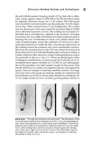
the perimeter is shown in Fig. 2-11. These are photographs taken
of disrupted metallization, as seen through the back side of an Al-
metallized fused quartz substrate [2-11 in SP]. In each photograph,
the bond parameters were held constant except for the power. Note
that the third bond (c), made at the highest US power, has cracked the
quartz. This is an example of cratering caused by excessive US energy
(see Chap. 8 for a discussion on cratering). Studies of evolution of the
bond interface on Au/Ni/Cu bond pads, obtained by etching the Al,
1% Si wedge bonds off, have revealed growth patterns similar to
FIGURE 2-11 “Through the underside of a bond pad.” The disruption of the
bond pad observed from the underside of a thin (~0.2 µm) evaporated Al
pad, which was deposited on a clear fused quartz substrate. These three
patterns were made by increasing the ultrasonic power for each Al wedge
bond, while holding force and time constant. Power-supply dial settings
were, from left to right, (a) 4.5; (b) 5.5; (c) 9.5. The third bond, made at
the highest US power, has cracked the quartz, an example of cratering
discussed in Chap. 8 [2-11].