
Page 198 - A Comprehensive Guide to Solar Energy Systems
P. 198
200 A COmPrehenSIVe GUIDe TO SOlAr enerGy SySTemS
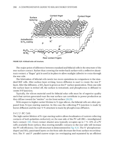
FIGURE 9.20 A bifacial solar cell structure.
The major point of difference between standard and bifacial cells is the structure of the
rear surface contact. rather than covering the entire back surface with a reflective alumi-
num contact, a “finger” grid is used in its place to allow sunlight (albedo) to come through
the rear side.
The fabrication of bifacial cells needs two more operations in comparison to the stan-
+
dard BSF cells. After surface layer etching, boron diffusion is used to create the rear P
+
layer. After the diffusion, a SiO 2 layer is grown as the P surface passivation. Then one side
the surface layer is etched off, the surface is texturized, and phosphorous is diffused to
create n P junction.
+
Typically, the silicon material used for bifacial solar cells must be of superior quality
such that carriers generated near the rear surface can contribute to power production as
they diffuse toward the “emitter” on the front surface [28,29].
With respect to higher carrier lifetime in n-type silicon, the bifacial cells are often pre-
pared from n-type starting material. In this case the collecting P n junction is made by
+
boron diffusion and the rear n n structure is made by phosphorous diffusion.
+
9.4.2.3 IBC Cells
The high carrier lifetime of n-type starting wafers allows localization of current collecting
contacts of both polarities exclusively on the rear side of the PV cell (IBC—interdigitated
back contact) [30]. Front contact shaded area typically occupies up to 7 %–10% of a PV
cell’s available front surface; thus moving metallic contacts to the rear side will increase
the PV cell efficiency. The cell structure is demonstrated in Fig. 9.21. The n phosphorous-
+
doped and SiO 2 -passivated layers on the front side decrease the front surface recombina-
tion. The n and P parallel narrow strips (no overlapping and separated by an efficient
+
+