
Page 196 - A Comprehensive Guide to Solar Energy Systems
P. 196
198 A COmPrehenSIVe GUIDe TO SOlAr enerGy SySTemS
thermally grown SiO 2 layer, in which some windows are opened. local boron diffusion
+
in these windows creates a local P back surface field. The Perl structure is shown in
Fig. 9.17B.
Both monocrystalline and multicrystalline boron-doped silicon contain relatively
high concentrations of oxygen. After illumination or carrier injection, B–O complexes
create recombination centers that result in severe carrier lifetime degradation, and con-
sequently, in a decrease in efficiency. The oxygen content limits the maximum efficiency
that is possible using P-type boron-doped silicon. The monocrystalline P-type silicon
prepared by the float zone method does not contain oxygen, and this type of solar cell
has the record efficiency of 24%. This material and fabrication technology (Perl [21]
prepared using microelectronic technology) is too expensive to be used in mass indus-
trial production.
9.4.2.2 PERT, TOPCon, and Bifacial Cells
Phosphorous-doped n-type silicon wafers retain lifetimes on the order of milliseconds
under the same stresses [22] and therefore can be used as a starting material for high-
efficient solar cells. The Pn junction is formed by boron diffusion [23]. A disadvantage of
this technology is that it needs a higher diffusion temperature than the phosphorous dif-
fusion and for P-type surface passivation there must be a layer of thermally grown SiO 2 , on
which a thin layer of Sin x :h or TiO 2 is deposited to form an effective antireflection coating.
This technology needs a process temperature of over 1000°C; this is also not compatible
with multicrystalline material because this material does not tolerate temperatures above
900°C [15]. Therefore, at present only monocrystalline starting n-type material is used in
this process for mass production. The multicrystalline n-type material cells technology
is still an object of research and development, even though recent research brings very
promising results [24].
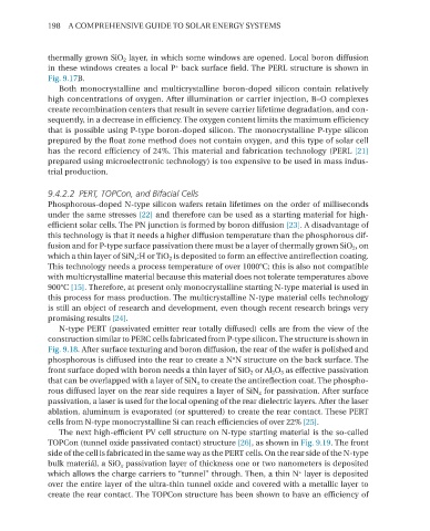
n-type PerT (passivated emitter rear totally diffused) cells are from the view of the
construction similar to PerC cells fabricated from P-type silicon. The structure is shown in
Fig. 9.18. After surface texturing and boron diffusion, the rear of the wafer is polished and
+
phosphorous is diffused into the rear to create a n n structure on the back surface. The
front surface doped with boron needs a thin layer of SiO 2 or Al 2 O 3 as effective passivation
that can be overlapped with a layer of Sin x to create the antireflection coat. The phospho-
rous diffused layer on the rear side requires a layer of Sin x for passivation. After surface
passivation, a laser is used for the local opening of the rear dielectric layers. After the laser
ablation, aluminum is evaporated (or sputtered) to create the rear contact. These PerT
cells from n-type monocrystalline Si can reach efficiencies of over 22% [25].
The next high-efficient PV cell structure on n-type starting material is the so-called
TOPCon (tunnel oxide passivated contact) structure [26], as shown in Fig. 9.19. The front
side of the cell is fabricated in the same way as the PerT cells. On the rear side of the n-type
bulk materiál, a SiO x passivation layer of thickness one or two nanometers is deposited
+
which allows the charge carriers to “tunnel” through. Then, a thin n layer is deposited
over the entire layer of the ultra-thin tunnel oxide and covered with a metallic layer to
create the rear contact. The TOPCon structure has been shown to have an efficiency of