
Page 192 - A Comprehensive Guide to Solar Energy Systems
P. 192
194 A COmPrehenSIVe GUIDe TO SOlAr enerGy SySTemS
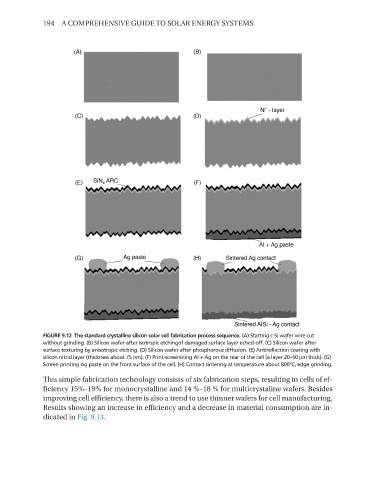
FIGURE 9.12 The standard crystalline silicon solar cell fabrication process sequence. (A) Starting c-Si wafer wire cut
without grinding. (B) Silicon wafer after isotropic etchingof damaged surface layer eched-off. (C) Silicon wafer after
surface texturing by anisotropic etching. (D) Silicon wafer after phosphorous diffusion. (E) Antireflection coating with
silicon nitrid layer (thickness about 75 nm). (F) Print-screenining Al + Ag on the rear of the cell (a layer 20–50 µm thick). (G)
Screen printing Ag paste on the front surface of the cell. (H) Contact sintering at temperature about 800°C, edge grinding.
This simple fabrication technology consists of six fabrication steps, resulting in cells of ef-
ficiency 15%–19% for monocrystalline and 14 %–18 % for multicrystaline wafers. Besides
improving cell efficiency, there is also a trend to use thinner wafers for cell manufacturing.
results showing an increase in efficiency and a decrease in material consumption are in-
dicated in Fig. 9.13.