
Page 187 - A Comprehensive Guide to Solar Energy Systems
P. 187
Chapter 9 • Crystalline Silicon Solar Cell and Module Technology 189
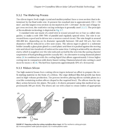
9.3.2 The Wafering Process
The silicon ingots (both single crystal and multicrystaline) have a cross section that is de-
termined by the final wafer size. At present the standard size is approximately 156 × 156
2
2
mm , and the largest cross section on the market is 210 × 210 mm . In the case of large in-
got cross sections, the multiwire cutting technique is generally used [2,3,7]. The principle
of the multiwire technology is depicted in Fig. 9.7.
A standard wire saw made of a steel wire is wound around two or four so-called wire-
guides, to make a web (500–700) of parallel and regularly spaced wires. The wire is un-
wound from a spool and is driven into a tension control circuit. The wire length is around
400–800 km, depending on its diameter (generally between 100 and 160 µm, but wire
diameters will be reduced in a few next years). The silicon ingot is glued to a substrate
holder (usually a glass plate glued to a steel plate) and then it is pushed against the moving
wire and sliced into hundreds of wafers at the same time. Cutting is achieved by an abrasive
slurry, which is supplied over the wire web and carried by the wire into the sawing channel
suspension of hard grinding particles (usually SiC). An alternative is using diamond plated
wires [9] in combination with the cooling liquid that allows approximately 3 times higher
cutting rate in comparison with slurry-based cutting. Diamond plated wire cutting is used
more for mono c-Si [4]. The kerf loss represents approximately 40% of c-Si material.
9.3.3 Ribbon Silicon
The high material losses from cutting silicon ingots induced an effort to prepare the mc-
Si starting material in the form of a ribbon. The edge-defined film-fed growth has been
used in high-volume production. The process involves placing silicon carbide plates in a
crucible-containing molten silicon (doped to the required level). The silicon rises by cap-
illary action between the plates. The poly c-Si sheets prepared using this method are ap-
proximately 300 µm thick. The sheets are cut with a laser to create wafers of appropriate
FIGURE 9.7 Preparing wafers by cutting crystalline silicon ingot. (A) The multiwire cutting principle.
(B) A monocrystalline wafer (pseudo-square). (C) A multicrystalline wafer.