
Page 188 - A Comprehensive Guide to Solar Energy Systems
P. 188
190 A COmPrehenSIVe GUIDe TO SOlAr enerGy SySTemS
dimensions. Details about this technology can be found in ref. [2]. Although ribbon solar
cell technology was expected to be very promising, at present it has become marginal and
represents less than 1% of world production [4].
9.4 Crystalline Silicon PV Cell Design and Fabrication
Technology
As described in this chapter, the cell design and fabrication processes have to maximize
power production from incoming irradiance and also minimize all kind of losses (optical,
recombination, and electrical) while the processing of materials and the techniques are
selected to minimize costs while maintaining a relatively high efficiency.
9.4.1 BSF Solar Cells
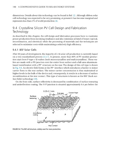
After 30 years of development, the majority of c-Si solar cell production is currently based
on a very standardized process [2,3,7]. At present, more than 80% of PV module produc-
tion start from P-type c-Si wafers (both monocrystalline and multicrystalline). These wa-
fers are made with a Pn junction over the entire front surface and a full-area aluminum-
+
based metallization with a PP structure on the rear. The design of this cell type is shown
+
in Fig. 9.8. An electric field forms at the PP interface which introduces a barrier to minor
carrier flows to the rear surface. The minor carrier concentration is thus maintained at
higher levels in the bulk of the device and, consequently, it results in a decrease of surface
recombination at the rear contact. This type of structures is known as the BSF (back sur-
face field) technology [10].
On the front side, surface reflectivity is decreased by combination of surface texturing
+
and antireflection coating. The n P junction is situated approximately 0.4 µm below the
FIGURE 9.8 The BSF cell structure, widely used for mass production.