
Page 189 - A Comprehensive Guide to Solar Energy Systems
P. 189
Chapter 9 • Crystalline Silicon Solar Cell and Module Technology 191
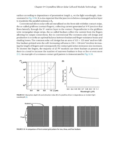
surface according to dependence of penetration length x l on the light wavelength, dem-
onstrated in Fig. 9.9A. It is also expected that the junction is below a damaged surface layer
to maximize the parallel resistance R p .
Conventional silicon solar cells are metallized on the front side withthin contact strips,
+
the so-called gridlines (contact fingers), collecting current generated at n P junction that
+
flows laterally through the n emitter layer to the contact. Perpendicular to the gridlines
wide rectangular-shape strips, the so-called busbars collect the current from the fingers
allowing for output connections. Key in conventional The common solar cell design and
production is to strike an optimal balance between busbar and finger resistance losses and
2
shading losses. The common solar cell design has an area of 125 × 125 mm and two full-
2
line busbars printed onto the cell. Increasing cell area to 156 × 156 mm involves increas-
ing the length of fingers and consequently the contact grid series resistance also increases.
To shorten the fingers, the majority of all PV modules use three busbars at present and
there is a trend to increase the number of narrower busbars to four or five or even more
[11]. An example of a common contact grid pattern is demonstrated in Fig. 9.10.
FIGURE 9.9 Absorption depth (A) and refraction index (B) of crystalline silicon in dependence on incident light
wavelength [3].
FIGURE 9.10 A comparison of front contact grid pattern for two, three, and four busbars.