
Page 190 - A Comprehensive Guide to Solar Energy Systems
P. 190
192 A COmPrehenSIVe GUIDe TO SOlAr enerGy SySTemS
The fabrication process for both monocrystalline and multicrystalline is almost the
same. At present, the most common thickness of wafers is 180 µm. The process has been
developed to avoid relatively high-cost operations like photolithography and vacuum de-
position techniques.
Initially, the wafers are etched in an isotropic chemical polishing etchant (e.g.,
hnO 3 :hF:Ch 3 COOh = 5:1:1) followed by washing in deionized water to remove surface
layers (approximately 10 µm) damaged during the cutting process. After removing the
damaged layer, wafers are anisotropic-etched to prepare the surface texturing.
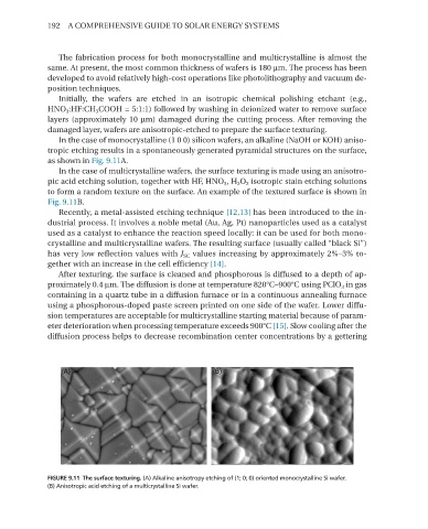
In the case of monocrystalline (1 0 0) silicon wafers, an alkaline (naOh or KOh) aniso-
tropic etching results in a spontaneously generated pyramidal structures on the surface,
as shown in Fig. 9.11A.
In the case of multicrystalline wafers, the surface texturing is made using an anisotro-
pic acid etching solution, together with hF, hnO 3 , h 2 O 2 isotropic stain etching solutions
to form a random texture on the surface. An example of the textured surface is shown in
Fig. 9.11B.
recently, a metal-assisted etching technique [12,13] has been introduced to the in-
dustrial process. It involves a noble metal (Au, Ag, Pt) nanoparticles used as a catalyst
used as a catalyst to enhance the reaction speed locally: it can be used for both mono-
crystalline and multicrystalline wafers. The resulting surface (usually called “black Si”)
has very low reflection values with J SC values increasing by approximately 2%–3% to-
gether with an increase in the cell efficiency [14].
After texturing, the surface is cleaned and phosphorous is diffused to a depth of ap-
proximately 0.4 µm. The diffusion is done at temperature 820°C–900°C using PClO 3 in gas
containing in a quartz tube in a diffusion furnace or in a continuous annealing furnace
using a phosphorous-doped paste screen printed on one side of the wafer. lower diffu-
sion temperatures are acceptable for multicrystalline starting material because of param-
eter deterioration when processing temperature exceeds 900°C [15]. Slow cooling after the
diffusion process helps to decrease recombination center concentrations by a gettering
FIGURE 9.11 The surface texturing. (A) Alkaline anisotropy etching of (1; 0; 0) oriented monocrystalline Si wafer.
(B) Anisotropic acid etching of a multicrystalline Si wafer.