
Page 195 - A Comprehensive Guide to Solar Energy Systems
P. 195
Chapter 9 • Crystalline Silicon Solar Cell and Module Technology 197
FIGURE 9.16 The MWT solar cells.
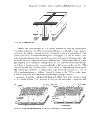
The PerC cell fabrication process is as follows. After surface texturing and phospho-
rous diffusion, the rear side of the wafer is polished followed by phosphor-silicate glass re-
moval and edge isolation. A thin layer Al 2 O 3 is deposited on the rear P-type surface (PeCVD
seems to be the best from the view of the process throughput [20]), and PeCVD Sin x (anti-
reflection coating) is deposited on the both front and rear surfaces. After deposition, a la-
ser is used for the local opening on the rear dielectric layers. After the laser ablation, screen
printing of Ag paste on the front and Al paste on the rear side with subsequent cofiring is
carried out to form the emitter contact and the local BSF contact on the rear side. PerC
cells can be fabricated from both mono c-Si and mc-Si. In comparison with the standard
BSF technology, it needs three more fabrication steps; this results in an increase of the cell
efficiency of approximately 1% (from 19% to 20%). At present, the PerC technology share
is approximately 10%, but is expected to increase significantly in future [4].
A similar cell structure with passivated rear side of the wafer is the passivated emit-
ter, rear locally diffused (Perl) structure. In this case, the rear surface is passivated with
FIGURE 9.17 PV cells with passivated emitter. (A) The PERC cell structure. (B) The PERL structure.