
Page 193 - A Comprehensive Guide to Solar Energy Systems
P. 193
Chapter 9 • Crystalline Silicon Solar Cell and Module Technology 195
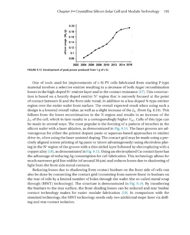
FIGURE 9.13 Development of peak power produced from 1 g of c-Si.
One of tools used for improvements of c-Si PV cells fabricated from starting P-type
material involves a selective emitter resulting in a decrease of both Auger recombination
+
losses in the high-doped n emitter layer and in the contact resistance [17]. This construc-
+
tion is based on a heavily doped emitter n region that is narrowly focused at the point
of contact between Si and the front side metal, in addition to a less doped n-type emitter
region over the entire wafer front surface. The overall expected result when using such a
design is a lowered overall value, as well as a slight increase of the J SC (from eq. 8.24). This
follows from the lower recombination in the n-region and results in an increase of the
J PV of the cell, which in turn results in a correspondingly higher V OC . Cells of this type can
be made in several ways. The most popular is the forming of a pattern of trenches in the
silicon wafer with a laser ablation, as demonstrated in Fig. 9.14. The laser grooves are ad-
vantageous for either the printed dopant paste or aqueous-based approaches to emitter
drive-in, often using the laser-assisted doping. The contact grid may be made using a pre-
cisely aligned screen printing of Ag paste or (more advantageously) using electroless plat-
+
ing in the n region of the groove with a thin nickel layer followed by electroplating with a
copper alloy [18], as demonstrated in Fig. 9.15. Using an electroplated Cu contact layer has
the advantage of reducing Ag consumption for cell fabrication. This technology allows for
much narrower grid line widths (of around 30 µm) and reduces losses due to shadowing of
light from the front side metal contacts.
reducing losses due to shadowing from contact busbars on the front side of cells can
also be done by connecting the contact grid (consisting from narrow lines) to busbars on
the rear of cells by a limited number of holes through the wafer [the so-called metal wrap
through (mWT) technology]. The structure is demonstrated in Fig. 9.16. By transferring
the busbars to the rear surface, the front shading losses can be reduced and rear busbar
contact technology makes for easier module fabrication [19]. In comparison with the
standard technology, the mWT technology needs only two additional steps: laser via drill-
ing and rear contact isolation.