
Page 199 - A Comprehensive Guide to Solar Energy Systems
P. 199
Chapter 9 • Crystalline Silicon Solar Cell and Module Technology 201
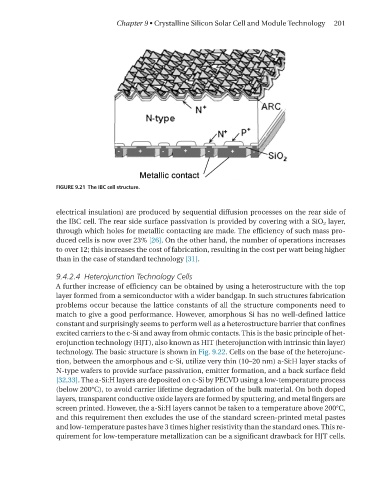
FIGURE 9.21 The IBC cell structure.
electrical insulation) are produced by sequential diffusion processes on the rear side of
the IBC cell. The rear side surface passivation is provided by covering with a SiO 2 layer,
through which holes for metallic contacting are made. The efficiency of such mass pro-
duced cells is now over 23% [26]. On the other hand, the number of operations increases
to over 12; this increases the cost of fabrication, resulting in the cost per watt being higher
than in the case of standard technology [31].
9.4.2.4 Heterojunction Technology Cells
A further increase of efficiency can be obtained by using a heterostructure with the top
layer formed from a semiconductor with a wider bandgap. In such structures fabrication
problems occur because the lattice constants of all the structure components need to
match to give a good performance. however, amorphous Si has no well-defined lattice
constant and surprisingly seems to perform well as a heterostructure barrier that confines
excited carriers to the c-Si and away from ohmic contacts. This is the basic principle of het-
erojunction technology (hJT), also known as hIT (heterojunction with intrinsic thin layer)
technology. The basic structure is shown in Fig. 9.22. Cells on the base of the heterojunc-
tion, between the amorphous and c-Si, utilize very thin (10–20 nm) a-Si:h layer stacks of
n-type wafers to provide surface passivation, emitter formation, and a back surface field
[32,33]. The a-Si:h layers are deposited on c-Si by PeCVD using a low-temperature process
(below 200°C), to avoid carrier lifetime degradation of the bulk material. On both doped
layers, transparent conductive oxide layers are formed by sputtering, and metal fingers are
screen printed. however, the a-Si:h layers cannot be taken to a temperature above 200°C,
and this requirement then excludes the use of the standard screen-printed metal pastes
and low-temperature pastes have 3 times higher resistivity than the standard ones. This re-
quirement for low-temperature metallization can be a significant drawback for hJT cells.