
Page 113 - An Introduction to Microelectromechanical Systems Engineering
P. 113
92 MEM Structures and Systems in Industrial and Automotive Applications
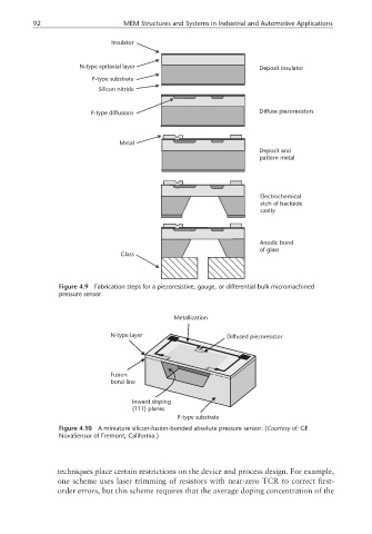
Insulator
N-type epitaxial layer Deposit insulator
P-type substrate
Silicon nitride
P-type diffusions Diffuse piezoresistors
Metal
Deposit and
pattern metal
Electrochemical
etch of backside
cavity
Anodic bond
of glass
Glass
Figure 4.9 Fabrication steps for a piezoresistive, gauge, or differential bulk micromachined
pressure sensor.
Metallization
N-type layer Diffused piezoresistor
Fusion
bond line
Inward sloping
{111} planes
P-type substrate
Figure 4.10 A miniature silicon-fusion-bonded absolute pressure sensor. (Courtesy of: GE
NovaSensor of Fremont, California.)
techniques place certain restrictions on the device and process design. For example,
one scheme uses laser trimming of resistors with near-zero TCR to correct first-
order errors, but this scheme requires that the average doping concentration of the