
Page 115 - An Introduction to Microelectromechanical Systems Engineering
P. 115
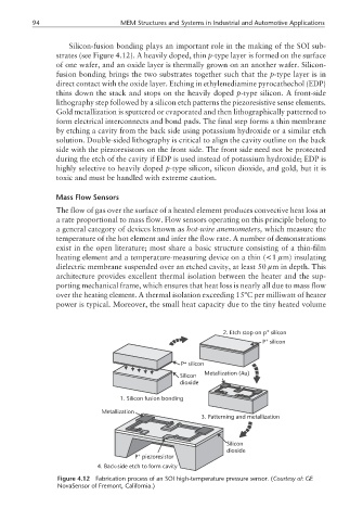
94                      MEM Structures and Systems in Industrial and Automotive Applications

                    Silicon-fusion bonding plays an important role in the making of the SOI sub-
                 strates (see Figure 4.12). A heavily doped, thin p-type layer is formed on the surface
                 of one wafer, and an oxide layer is thermally grown on an another wafer. Silicon-
                 fusion bonding brings the two substrates together such that the p-type layer is in
                 direct contact with the oxide layer. Etching in ethylenediamine pyrocathechol (EDP)
                 thins down the stack and stops on the heavily doped p-type silicon. A front-side
                 lithography step followed by a silicon etch patterns the piezoresistive sense elements.
                 Gold metallization is sputtered or evaporated and then lithographically patterned to
                 form electrical interconnects and bond pads. The final step forms a thin membrane
                 by etching a cavity from the back side using potassium hydroxide or a similar etch
                 solution. Double-sided lithography is critical to align the cavity outline on the back
                 side with the piezoresistors on the front side. The front side need not be protected
                 during the etch of the cavity if EDP is used instead of potassium hydroxide; EDP is
                 highly selective to heavily doped p-type silicon, silicon dioxide, and gold, but it is
                 toxic and must be handled with extreme caution.


                 Mass Flow Sensors
                 The flow of gas over the surface of a heated element produces convective heat loss at
                 a rate proportional to mass flow. Flow sensors operating on this principle belong to
                 a general category of devices known as hot-wire anemometers, which measure the
                 temperature of the hot element and infer the flow rate. A number of demonstrations
                 exist in the open literature; most share a basic structure consisting of a thin-film
                 heating element and a temperature-measuring device on a thin (<1 µm) insulating
                 dielectric membrane suspended over an etched cavity, at least 50 µm in depth. This
                 architecture provides excellent thermal isolation between the heater and the sup-
                 porting mechanical frame, which ensures that heat loss is nearly all due to mass flow
                 over the heating element. A thermal isolation exceeding 15ºC per milliwatt of heater
                 power is typical. Moreover, the small heat capacity due to the tiny heated volume


                                                                           +
                                                               2. Etch stop on p silicon
                                                                           +
                                                                          P silicon
                                                    +
                                                   P silicon
                                                          Metallization (Au)
                                                   Silicon
                                                   dioxide
                                  1. Silicon fusion bonding

                             Metallization
                                                         3. Patterning and metallization


                                                                Silicon
                                                                dioxide
                                       +
                                      P piezoresistor
                            4. Back-side etch to form cavity
                 Figure 4.12  Fabrication process of an SOI high-temperature pressure sensor. (Courtesy of: GE
                 NovaSensor of Fremont, California.)