
Page 155 - Analog and Digital Filter Design
P. 155
1 52 Analog and Digital Filter Design
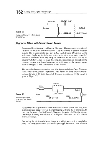
Rs=l50 C2=34.713nF
I II
II
Source
Figure 5.6
L1=1.4619mH L3=Om7778mH
Highpass Filter with Infinite Load
Impedance
Highpass Filters with Transmission Zeroes
Cauer (or elliptic function) and Inverse Chebyshev filters are more complicated
than the ladder filters already described. They have series or parallel resonant
circuits. The lowpass model can have either parallel tuned LC circuits in the
series arms (replacing the inductors in the ladder circuit) or series tuned LC
circuits in the shunt arms (replacing the capacitors in the ladder circuit). In
Chapter 4, I showed that the same denormalizing equations can be used for the
resonant circuits; now I am also converting to highpass, so the element values
must be swapped as well. An example of this follows.
The normalized component values for a 0.1 dB passband ripple Cauer filter were
taken from a table given in Stephenson.' This circuit has 30dB stopband atten-
uation, starting at 2.5 times the cutoff frequency; a diagram of the circuit is
given in Figure 5.7.
II output
II
Figure 5.7 Input C2=0.12049 R2=1
Normalized Cauer
Lowpass Filter, 1 rad/s
cutoff
An alternative design uses two series inductors between source and load, with
a series resonant circuit between their connecting node and the common rail. In
that case the value of L2 in Figure 5.7 becomes the value of C2 in the alterna-
tive design. Similarly, the value of C2 in Figure 5.7 becomes that of L2 in the
alternative design.
Converting the minimum inductor design into a highpass circuit is straightfor-
ward. The shunt capacitor of the lowpass prototype becomes a shunt inductor