
Page 355 - Complete Wireless Design
P. 355
Support Circuit Design
354 Chapter Eight
return for DC. R ’s value will normally be about 68 ohms. A small-signal
1
square-law power detector circuit will replace R with an RFC. R serves as the
1 2
load resistor for the RC time constant of the detector, and can be anywhere
from 1 kilohm for the large-signal envelope detector to 5 kilohms for the small-
signal square-law power detector (the difference between the two types of
detectors is explained below). The DC OUTPUT should be placed into a high
input impedance op-amp, or the DC output voltage will drop below expecta-
tions, since in designing an unbiased detector circuit (especially for square-law
detector operation) the diode’s junction resistance can be up to a few thousand
ohms. Any Schottky detector’s sensitivity will depend on the detector’s load
being much greater than the diode’s internal resistance (R ), so the input resis-
J
tance of the next stage should be higher than 75 kilohms. Because of this high
R value, input LC matching into the diode is rarely attempted.
J
The zero-bias Schottky diode should be chosen if small RF inputs are
expected, since they will be much less sensitive to temperature variations than
a biased diode arrangement (the detector’s sensitivity is a measure of the input
signal’s amplitude compared to the output amplitude of the detector, measured
in mV/ W, with higher values being better). Biased diodes have been employed
to detect low signal levels in the past, as the detector circuit sensitivity can be
dramatically improved by using a DC voltage to bias the diode to a point just
before it begins to solidly conduct (0.7 V for silicon). This allows for less of an
IF input amplitude before the diode strongly detects the signal. However, usu-
ally Schottky diodes need a small bias, even the “zero bias” types, when detect-
ing very low amplitude RF signals. If not, then most of the RF signal’s power
will be dropped across the high junction resistance of the diode, and very little
across the desired load resistance, unless the load resistance is made to be of a
very high value.
As inferred above, Schottky diode detectors will detect power, since they
operate in their square-law region at small signal input levels; high input lev-
els will change the diode’s response to peak voltage detection. So two basic
types of detectors are utilized in RF circuits: the envelope detector and the
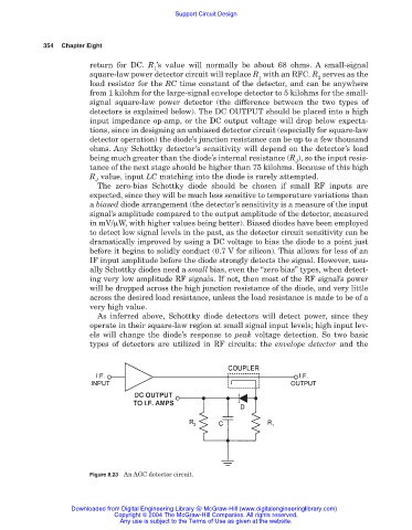
Figure 8.23 An AGC detector circuit.
Downloaded from Digital Engineering Library @ McGraw-Hill (www.digitalengineeringlibrary.com)
Copyright © 2004 The McGraw-Hill Companies. All rights reserved.
Any use is subject to the Terms of Use as given at the website.