
Page 352 - Complete Wireless Design
P. 352
Support Circuit Design
Support Circuit Design 351
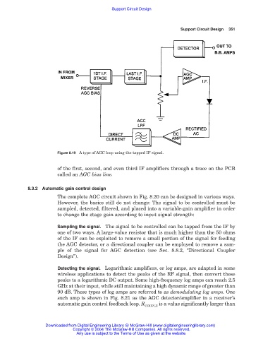
Figure 8.19 A type of AGC loop using the tapped IF signal.
of the first, second, and even third IF amplifiers through a trace on the PCB
called an AGC bias line.
8.3.2 Automatic gain control design
The complete AGC circuit shown in Fig. 8.20 can be designed in various ways.
However, the basics still do not change: The signal to be controlled must be
sampled, detected, filtered, and placed into a variable-gain amplifier in order
to change the stage gain according to input signal strength:
Sampling the signal. The signal to be controlled can be tapped from the IF by
one of two ways. A large-value resistor that is much higher than the 50 ohms
of the IF can be exploited to remove a small portion of the signal for feeding
the AGC detector, or a directional coupler can be employed to remove a sam-
ple of the signal for AGC detection (see Sec. 8.8.2, “Directional Coupler
Design”).
Detecting the signal. Logarithmic amplifiers, or log amps, are adapted in some
wireless applications to detect the peaks of the RF signal, then convert these
peaks to a logarithmic DC output. Some high-frequency log amps can reach 2.5
GHz at their input, while still maintaining a high dynamic range of greater than
90 dB. These types of log amps are referred to as demodulating log amps. One
such amp is shown in Fig. 8.21 as the AGC detector/amplifier in a receiver’s
automatic gain control feedback loop. R is a value significantly larger than
COUPLE
Downloaded from Digital Engineering Library @ McGraw-Hill (www.digitalengineeringlibrary.com)
Copyright © 2004 The McGraw-Hill Companies. All rights reserved.
Any use is subject to the Terms of Use as given at the website.