
Page 348 - Complete Wireless Design
P. 348
Support Circuit Design
Support Circuit Design 347
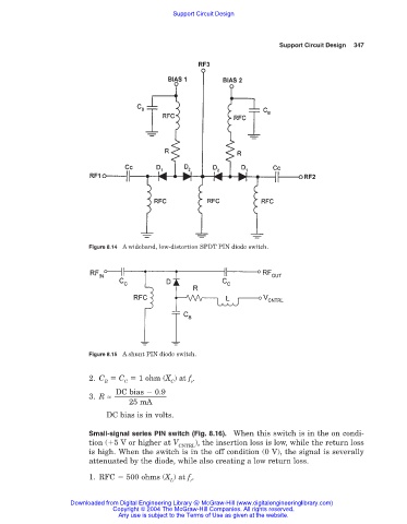
Figure 8.14 A wideband, low-distortion SPDT PIN diode switch.
Figure 8.15 A shunt PIN diode switch.
2. C C 1 ohm (X ) at f .
B C C r
DC bias 0.9
3. R ≈
25 mA
DC bias is in volts.
Small-signal series PIN switch (Fig. 8.16). When this switch is in the on condi-
tion ( 5 V or higher at V ), the insertion loss is low, while the return loss
CNTRL
is high. When the switch is in the off condition (0 V), the signal is severally
attenuated by the diode, while also creating a low return loss.
1. RFC 500 ohms (X ) at f .
L r
Downloaded from Digital Engineering Library @ McGraw-Hill (www.digitalengineeringlibrary.com)
Copyright © 2004 The McGraw-Hill Companies. All rights reserved.
Any use is subject to the Terms of Use as given at the website.