
Page 349 - Complete Wireless Design
P. 349
Support Circuit Design
348 Chapter Eight
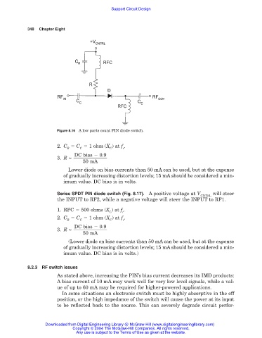
Figure 8.16 A low parts count PIN diode switch.
2. C C 1 ohm (X ) at f .
B C C r
DC bias 0.9
3. R ≈
50 mA
Lower diode on bias currents than 50 mA can be used, but at the expense
of gradually increasing distortion levels; 15 mA should be considered a min-
imum value. DC bias is in volts.
Series SPDT PIN diode switch (Fig. 8.17). A positive voltage at V will steer
CNTRL
the INPUT to RF2, while a negative voltage will steer the INPUT to RF1.
1. RFC 500 ohms (X ) at f .
L r
2. C C 1 ohm (X ) at f .
B C C r
DC bias 0.9
3. R ≈
50 mA
(Lower diode on bias currents than 50 mA can be used, but at the expense
of gradually increasing distortion levels; 15 mA should be considered a min-
imum value. DC bias is in volts.)
8.2.3 RF switch issues
As stated above, increasing the PIN’s bias current decreases its IMD products:
A bias current of 10 mA may work well for very low level signals, while a val-
ue of up to 60 mA may be required for higher-powered applications.
In some situations an electronic switch must be highly absorptive in the off
position, or the high impedance of the switch will cause the power at its input
to be reflected back to the source. This can severely degrade circuit perfor-
Downloaded from Digital Engineering Library @ McGraw-Hill (www.digitalengineeringlibrary.com)
Copyright © 2004 The McGraw-Hill Companies. All rights reserved.
Any use is subject to the Terms of Use as given at the website.