
Page 353 - Complete Wireless Design
P. 353
Support Circuit Design
352 Chapter Eight
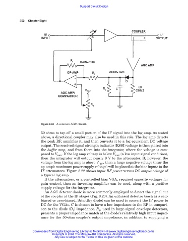
Figure 8.20 A common AGC circuit.
50 ohms to tap off a small portion of the IF signal into the log amp. As stated
above, a directional coupler may also be used in this role. The log amp detects
the peak RF, amplifies it, and then converts it to a log equivalent DC voltage
output. The received signal strength indicator (RSSI) voltage is then placed into
the buffer amp, and from there into the integrator, where the voltage is com-
pared to V . If the log amp voltage is below V (a low input signal condition),
REF REF
then the integrator will output nearly 0 V to the attenuator. If, however, the
voltage from the log amp is above V , then a large negative voltage (near the
REF
op-amp’s maximum power supply voltage) will be placed at the bias inputs to the
IF attenuators. Figure 8.22 shows input RF power versus DC output voltage of
a typical log amp.
If the attenuators, or a controlled bias VGA, required opposite voltages for
gain control, then an inverting amplifier can be used, along with a positive
supply voltage for the integrator.
An AGC detector diode is more commonly employed to detect the signal out
of the coupler at the IF stages (Fig. 8.23). An unbiased detector (such as a self-
biased or zero-biased, Schottky diode) can be used to convert the IF power to
DC for the VGAs. C is chosen to have a low impedance to the RF in compari-
son to the diode (D ) impedance. R , used in large-signal envelope detectors,
1 1
presents a proper impedance match at the diode’s relatively high input imped-
ance for the 50-ohm coupler’s output impedance, in addition to supplying a
Downloaded from Digital Engineering Library @ McGraw-Hill (www.digitalengineeringlibrary.com)
Copyright © 2004 The McGraw-Hill Companies. All rights reserved.
Any use is subject to the Terms of Use as given at the website.