
Page 351 - Complete Wireless Design
P. 351
Support Circuit Design
350 Chapter Eight
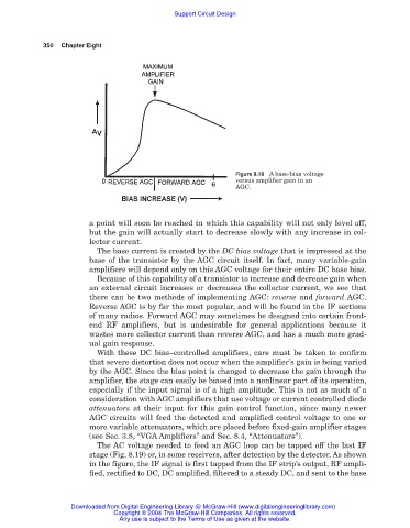
Figure 8.18 A base-bias voltage
versus amplifier gain in an
AGC.
a point will soon be reached in which this capability will not only level off,
but the gain will actually start to decrease slowly with any increase in col-
lector current.
The base current is created by the DC bias voltage that is impressed at the
base of the transistor by the AGC circuit itself. In fact, many variable-gain
amplifiers will depend only on this AGC voltage for their entire DC base bias.
Because of this capability of a transistor to increase and decrease gain when
an external circuit increases or decreases the collector current, we see that
there can be two methods of implementing AGC: reverse and forward AGC.
Reverse AGC is by far the most popular, and will be found in the IF sections
of many radios. Forward AGC may sometimes be designed into certain front-
end RF amplifiers, but is undesirable for general applications because it
wastes more collector current than reverse AGC, and has a much more grad-
ual gain response.
With these DC bias–controlled amplifiers, care must be taken to confirm
that severe distortion does not occur when the amplifier’s gain is being varied
by the AGC. Since the bias point is changed to decrease the gain through the
amplifier, the stage can easily be biased into a nonlinear part of its operation,
especially if the input signal is of a high amplitude. This is not as much of a
consideration with AGC amplifiers that use voltage or current controlled diode
attenuators at their input for this gain control function, since many newer
AGC circuits will feed the detected and amplified control voltage to one or
more variable attenuators, which are placed before fixed-gain amplifier stages
(see Sec. 3.8, “VGA Amplifiers” and Sec. 8.4, “Attenuators”).
The AC voltage needed to feed an AGC loop can be tapped off the last IF
stage (Fig. 8.19) or, in some receivers, after detection by the detector. As shown
in the figure, the IF signal is first tapped from the IF strip’s output, RF ampli-
fied, rectified to DC, DC amplified, filtered to a steady DC, and sent to the base
Downloaded from Digital Engineering Library @ McGraw-Hill (www.digitalengineeringlibrary.com)
Copyright © 2004 The McGraw-Hill Companies. All rights reserved.
Any use is subject to the Terms of Use as given at the website.