
Page 346 - Complete Wireless Design
P. 346
Support Circuit Design
Support Circuit Design 345
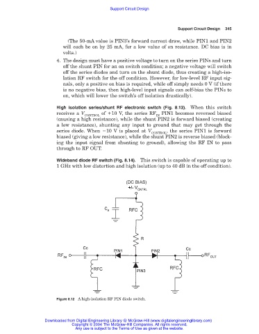
(The 50-mA value is PIN3’s forward current draw, while PIN1 and PIN2
will each be on by 25 mA, for a low value of on resistance. DC bias is in
volts.)
4. The design must have a positive voltage to turn on the series PINs and turn
off the shunt PIN for an on switch condition; a negative voltage will switch
off the series diodes and turn on the shunt diode, thus creating a high-iso-
lation RF switch for the off condition. However, for low-level RF input sig-
nals, only a positive on bias is required, while off simply needs 0 V (if there
is no negative bias, then high-level input signals can self-bias the PINs to
on, which will lower the switch’s off isolation drastically).
High isolation series/shunt RF electronic switch (Fig. 8.13). When this switch
receives a V of 10 V, the series RF PIN1 becomes reversed biased
CONTROL IN
(causing a high resistance), while the shunt PIN2 is forward biased (creating
a low resistance), shunting any input to ground that may get through the
series diode. When 10 V is placed at V , the series PIN1 is forward
CONTROL
biased (giving a low resistance), while the shunt PIN2 is reverse biased (block-
ing the input signal from shunting to ground), allowing the RF IN to pass
through to RF OUT.
Wideband diode RF switch (Fig. 8.14). This switch is capable of operating up to
1 GHz with low distortion and high isolation (up to 40 dB in the off condition).
Figure 8.12 A high-isolation RF PIN diode switch.
Downloaded from Digital Engineering Library @ McGraw-Hill (www.digitalengineeringlibrary.com)
Copyright © 2004 The McGraw-Hill Companies. All rights reserved.
Any use is subject to the Terms of Use as given at the website.