
Page 342 - Complete Wireless Design
P. 342
Support Circuit Design
Support Circuit Design 341
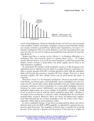
Figure 8.7 Subharmonics and
harmonics of a multiplier stage.
action of multiplication. However, Schottky diodes will not have this increased
noise problem: Doubler and tripler topologies using low-noise Schottky diodes
can usually maintain a good 20 log N phase noise degradation, even up to 7.
Varactor multipliers (Fig. 8.8) can be delicate to tune for top performance, but
they too add very low levels of phase and amplitude noise beyond the unavoid-
able 20 log N.
Diodes must have a certain carrier lifetime ( ) to function efficiently as a
multiplier. This value must be equal to or greater than /(1/f ) 10. Longer
IN
carrier lifetime factors of up to 30 are more beneficial in that they permit the
diode’s reverse current to peak before the diode rapidly travels back to its
high-impedance condition.
As mentioned, DC biasing a diode multiplier assists it in the frequency mul-
tiplication process. But because the diode of a simple frequency multiplier rec-
tifies a certain amount of the RF, a resistor placed in shunt with the multiplier
diode will furnish the necessary negative DC bias voltage. However, a small
external negative DC bias voltage source can be used across the diode as
required.
Transistor (Class C or B) frequency multipliers will have acceptable output
noise levels, conversion gain, and bandwidth. Active multipliers can also con-
sume less DC current than many diode multipliers because of the sometimes
necessary inclusion of Class A amplifiers in a lossy diode multiplier chain to
increase its output power. Additionally, any cascading of multiple varactor
multiplier stages opens up a severe danger of instability (oscillations), which
is not as much of a risk as with the active multiplier types. Still, a doubler is
the safest active multiplier to construct, while cascading them for any further
multiplication required. However, there are many low-phase-noise applica-
tions that demand the use of diode multipliers over the noisier active type—
especially within digital communication radios.
In active multiplier design, it has been recommended by Maas and others
that the duty cycle of a BJT or FET amplifier be adjusted to optimize the pre-
ferred output harmonic. The amplifier is biased close to cutoff to be on for 30
percent of the time for a doubler and 20 percent of the time for a tripler. In
Downloaded from Digital Engineering Library @ McGraw-Hill (www.digitalengineeringlibrary.com)
Copyright © 2004 The McGraw-Hill Companies. All rights reserved.
Any use is subject to the Terms of Use as given at the website.