
Page 347 - Complete Wireless Design
P. 347
Support Circuit Design
346 Chapter Eight
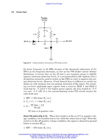
Figure 8.13 A high-isolation series/shunt PIN diode switch.
Its lower frequency is 50 MHz because of the decreased inductance of the
RFCs as the frequency decreases, as well as the PIN diode’s carrier lifetime
limitations. A reverse bias on the off arm is not required, except to slightly
improve harmonic distortion levels. It is recommended by HP (Agilent) that a
40-mA bias current be used to switch on the PINs in order to improve the out-
put distortion levels. However, 15-mA forward bias is sufficient to switch the
diodes on with minimal, but not optimal, distortion of the signal. For switch-
ing low-level amplitude input signals from a receiver, BIAS 1 and BIAS 2
need only be 5 and 0 V. For higher power signals, the bias should be 5 V
(on) and 5 V (off). R is the current-limiting series PIN switch resistor for
each diode pair.
1. RFC 500 ohms (X ) at f .
L r
2. C C 1 ohm (X ) at f .
B C C r
DC bias 0.9
3. R ≈
80 mA
DC bias is in positive volts.
Shunt PIN switch (Fig. 8.15). When this switch is in the on (0 V or negative volt-
age) condition, the insertion loss is low, while the return loss is high. When the
switch is in the off (positive voltage) condition, the signal is shunted to ground
before it reaches RF .
OUT
1. RFC 500 ohms (X ) at f .
L r
Downloaded from Digital Engineering Library @ McGraw-Hill (www.digitalengineeringlibrary.com)
Copyright © 2004 The McGraw-Hill Companies. All rights reserved.
Any use is subject to the Terms of Use as given at the website.