
Page 350 - Complete Wireless Design
P. 350
Support Circuit Design
Support Circuit Design 349
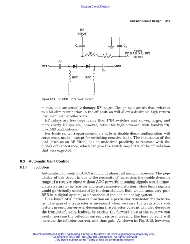
Figure 8.17 An SPDT PIN diode switch.
mance, and can actually damage RF stages. Designing a switch that switches
to a 50-ohm termination in the off position will allow a desirable high return
loss, minimizing reflections.
RF relays are less dependable than PIN switches and slower, larger, and
more costly. Relays are, however, better for high-powered, wide bandwidth,
low-IMD applications.
For basic switch requirements, a single or double diode configuration will
serve most needs—except for switching reactive loads. The inductance of the
load (such as an RF filter), has an undesired proclivity to resonate with the
diode’s off capacitance, which can give the switch very little of the off isolation
that was expected.
8.3 Automatic Gain Control
8.3.1 Introduction
Automatic gain control (AGC) is found in almost all modern receivers. The pop-
ularity of this circuit is due to the necessity of increasing the usable dynamic
range of a receiver, since without AGC powerful incoming signals would imme-
diately saturate the receiver and create massive distortion, while feeble signals
would go virtually undetected by the demodulator. Both would cause very poor
BER in a digital system, or unreadable signals in an analog system.
Bias-based AGC networks function on a particular transistor characteris-
tic: The gain of a transistor is increased when we raise the transistor’s col-
lector current; conversely, decreasing the collector current will also decrease
the transistor’s gain. Indeed, by raising the forward bias at the base we can
easily increase the collector current, since increasing the base current will
increase the collector current, and thus gain. As shown in Fig. 8.18, however,
Downloaded from Digital Engineering Library @ McGraw-Hill (www.digitalengineeringlibrary.com)
Copyright © 2004 The McGraw-Hill Companies. All rights reserved.
Any use is subject to the Terms of Use as given at the website.