
Page 343 - Complete Wireless Design
P. 343
Support Circuit Design
342 Chapter Eight
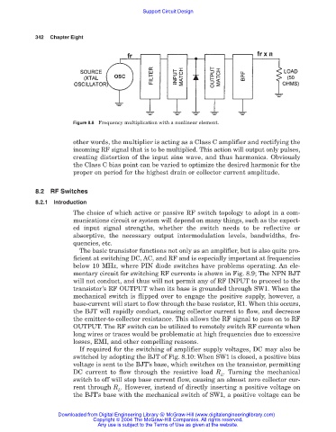
Figure 8.8 Frequency multiplication with a nonlinear element.
other words, the multiplier is acting as a Class C amplifier and rectifying the
incoming RF signal that is to be multiplied. This action will output only pulses,
creating distortion of the input sine wave, and thus harmonics. Obviously
the Class C bias point can be varied to optimize the desired harmonic for the
proper on period for the highest drain or collector current amplitude.
8.2 RF Switches
8.2.1 Introduction
The choice of which active or passive RF switch topology to adopt in a com-
munications circuit or system will depend on many things, such as the expect-
ed input signal strengths, whether the switch needs to be reflective or
absorptive, the necessary output intermodulation levels, bandwidths, fre-
quencies, etc.
The basic transistor functions not only as an amplifier, but is also quite pro-
ficient at switching DC, AC, and RF and is especially important at frequencies
below 10 MHz, where PIN diode switches have problems operating. An ele-
mentary circuit for switching RF currents is shown in Fig. 8.9; The NPN BJT
will not conduct, and thus will not permit any of RF INPUT to proceed to the
transistor’s RF OUTPUT when its base is grounded through SW1. When the
mechanical switch is flipped over to engage the positive supply, however, a
base-current will start to flow through the base resistor, R1. When this occurs,
the BJT will rapidly conduct, causing collector current to flow, and decrease
the emitter-to-collector resistance. This allows the RF signal to pass on to RF
OUTPUT. The RF switch can be utilized to remotely switch RF currents when
long wires or traces would be problematic at high frequencies due to excessive
losses, EMI, and other compelling reasons.
If required for the switching of amplifier supply voltages, DC may also be
switched by adopting the BJT of Fig. 8.10: When SW1 is closed, a positive bias
voltage is sent to the BJT’s base, which switches on the transistor, permitting
DC current to flow through the resistive load R . Turning the mechanical
L
switch to off will stop base current flow, causing an almost zero collector cur-
rent through R . However, instead of directly inserting a positive voltage on
L
the BJT’s base with the mechanical switch of SW1, a positive voltage can be
Downloaded from Digital Engineering Library @ McGraw-Hill (www.digitalengineeringlibrary.com)
Copyright © 2004 The McGraw-Hill Companies. All rights reserved.
Any use is subject to the Terms of Use as given at the website.