
Page 344 - Complete Wireless Design
P. 344
Support Circuit Design
Support Circuit Design 343
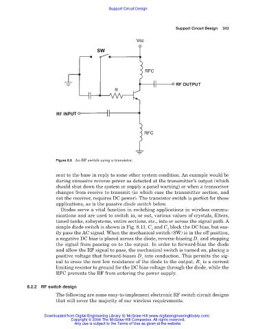
Figure 8.9 An RF switch using a transistor.
sent to the base in reply to some other system condition. An example would be
during excessive reverse power as detected at the transmitter’s output (which
should shut down the system or supply a panel warning) or when a transceiver
changes from receive to transmit (in which case the transmitter section, and
not the receiver, requires DC power). The transistor switch is perfect for these
applications, as is the passive diode switch below.
Diodes serve a vital function in switching applications in wireless commu-
nications and are used to switch in, or out, various values of crystals, filters,
tuned tanks, subsystems, entire sections, etc., into or across the signal path. A
simple diode switch is shown in Fig. 8.11. C and C block the DC bias, but eas-
1 2
ily pass the AC signal. When the mechanical switch (SW) is in the off position,
a negative DC bias is placed across the diode, reverse-biasing D and stopping
1
the signal from passing on to the output. In order to forward-bias the diode
and allow the RF signal to pass, the mechanical switch is turned on, placing a
positive voltage that forward-biases D into conduction. This permits the sig-
1
nal to cross the now low resistance of the diode to the output. R is a current
1
limiting resistor to ground for the DC bias voltage through the diode, while the
RFC prevents the RF from entering the power supply.
8.2.2 RF switch design
The following are some easy-to-implement electronic RF switch circuit designs
that will cover the majority of our wireless requirements.
Downloaded from Digital Engineering Library @ McGraw-Hill (www.digitalengineeringlibrary.com)
Copyright © 2004 The McGraw-Hill Companies. All rights reserved.
Any use is subject to the Terms of Use as given at the website.